PCB Antenna Design and Fabrication
R2026bUse Antenna Toolbox™ to design custom printed circuit board (PCB) antennas for practical designs such as cell phones, RFID, and IoT applications. Prototype and implement simulated PCB antennas by specifying the RF connector suitable for your application and customizing the PCB manufacturing services.
Combine geometrical shapes and mathematical operations to create
unique antenna geometries that meet for your antenna specifications. For
example, you can use the shape objects and their functions to create
single or multi-layered PCB-based antenna designs using the pcbStack object.
Use PCB fabrication objects and functions in this category to read and write (PCB) designs using Gerber files.
To interactively design, analyze, and export single or multi-feed PCB antennas, use the PCB Antenna Designer app.
Apps
| PCB Antenna Designer | Design, analyze, optimize, and export single or multifeed PCB antennas |
Objects
Functions
Topics
- PCB Feeds
Basics of PCB signal feeds, including feed type definitions and applications of each feed type. (Since R2026b)
- Board Thickness versus Dielectric Thickness in PCB
Define board and dielectric thickness of a PCB antenna for various scenarios like single and multi-layer dielectric, and imported designs from Gerber files. (Since R2022b)
Featured Examples
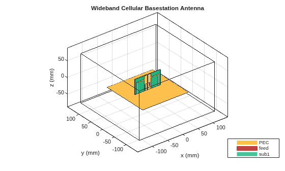
Design Wideband Cellular Base Station Antenna with Parasitic Elements
Design a custom antenna with parasitic elements to enhance its directivity and bandwidth for cellular base station applications.
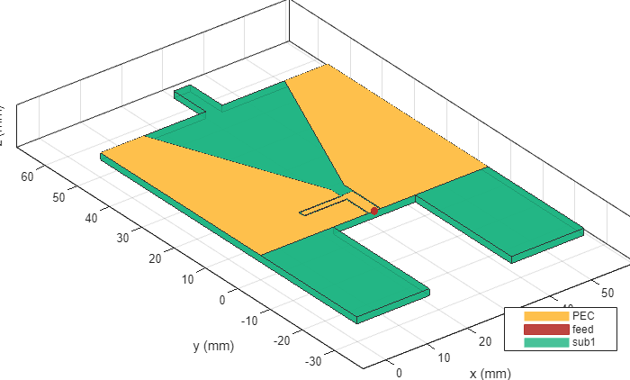
Modeling and Analysis of 5G NR FR1 Ultra-Wideband Antenna
Model a 5G NR FR1 Ultra-wideband antenna having a coplanar structure with no ground plane and an arbitrary finite gap feed.

Model Coaxial Gap Feed for Probe-Fed Patch Antenna
Comparison of a standard delta-gap probe feed model and a finite-gap coaxial feed model for a patch antenna.
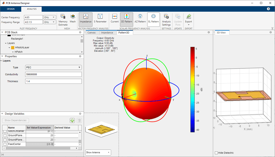
Design and Analysis Using PCB Antenna Designer
Design, validate, analyze, and export 1-by-2 H-notch linear antenna array.
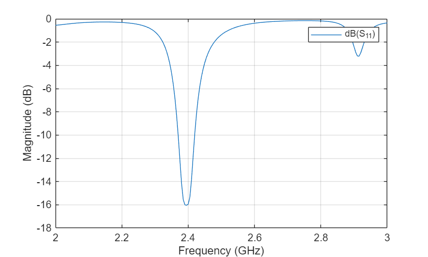
Dual-Fed Square Microstrip Patch Antenna for BLE Applications
Design and analyze the dual-fed square microstrip patch antenna for Bluetooth Low Energy applications.
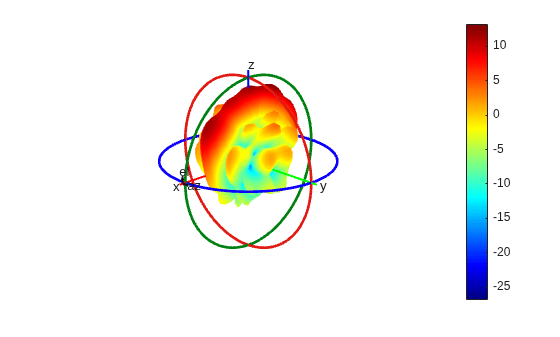
Corporate Feed Divider Network for a Linear Patch Antenna Array
Integrate a corporate power divider with a microstrip patch antenna array to provide a signal feed to the antenna array. Corporate power dividers are used to divide, or combine, RF signals, either equally or unequally, from one port to multiple ports. The corporate power divider is available as a catalog element in RF PCB Toolbox™. The patch antenna array is built using the patchMicrostripInsetfed catalog element and pcbStack from Antenna Toolbox™.
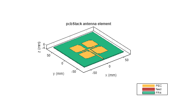
Design, Analyze, and Prototype 2-by-2 Patch Antenna Array
Design and analysis of a 2‑by‑2 microstrip patch antenna array on an FR4 substrate operating at 2.4 GHz, including full simulation and generation of PCB Gerber files for fabrication.
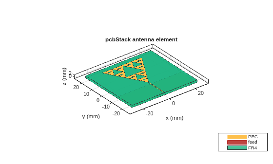
Modified Sierpinski Monopole Fractal Antenna for Dual-Band Application
Model and analyze a compact second‑order modified Sierpinski fractal monopole antenna on an FR4 substrate for dual‑band S‑ and C‑band operation.
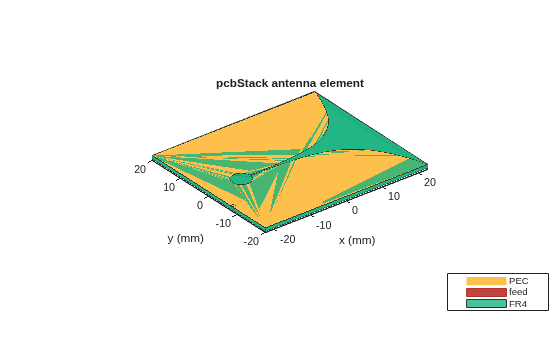
Create Antenna Model from Gerber Files
Create an antenna model from Gerber files and subsequently analyze the antenna. The Gerber file format is used in printed circuit board (PCB) manufacturing and is defined in the RS-274X standard which is the newer extended Gerber format. The Antenna Toolbox™ supports the newer RS-274X format both to generate Gerber files from an antenna model as well as to create an antenna model from a set of Gerber files.
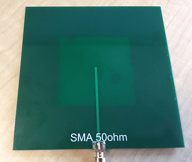
Design, Analysis, and Prototyping of Microstrip-Fed Wide-Slot Antenna
Model a microstrip-fed printed wide slot antenna with an FR4 substrate, analyze it, and finally generate Gerber files to enable its prototyping. The design is intended for operation in the L-band and has a bandwidth of about 17% over the band 1.6 - 1.8 GHz.
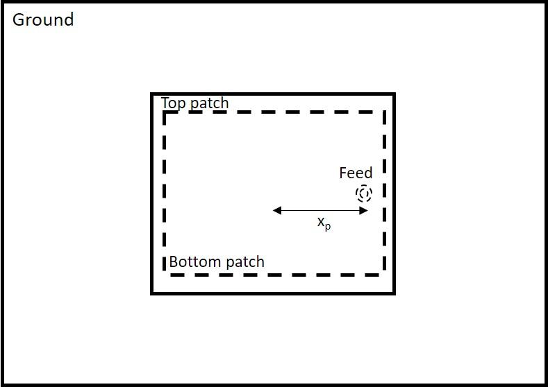
Modeling and Analysis of Probe-Fed Stacked Patch Antenna
The steps to model and analyze a probe-fed stacked patch antenna. The standard rectangular microstrip patch antenna has a narrow impedance bandwidth typically less than 5%. The stacked patch configuration is one of the ways of increasing the impedance bandwidth of these antennas to be greater than 25% [1]. There are different ways of designing stacked patches, primarily differing in the way their feed is designed [2]. The two types of feeding mechanisms are probe-feed and aperture coupled. These two mechanisms have a role in the impedance bandwidth behavior as well as the radiation characteristics of the antenna.
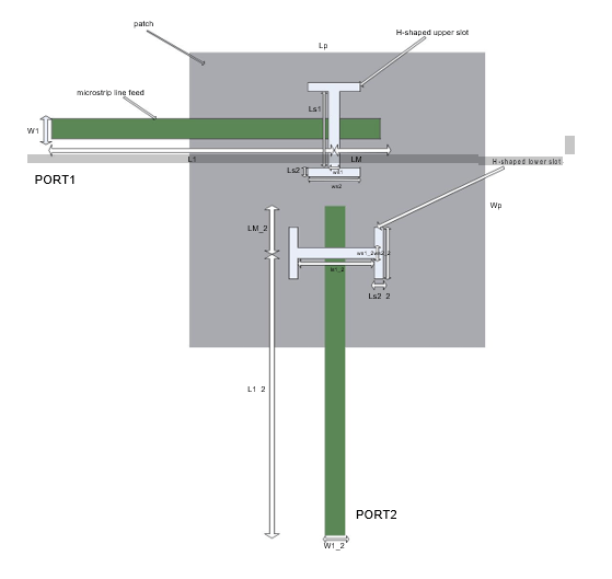
Model and Analyze Dual Polarized Patch Microstrip Antenna
Design and measure a wideband dual polarized microstrip antenna that finds its use at the base station of a cellular system. In order to achieve the wideband characteristics, this design considers a slot coupled patch antenna structure.
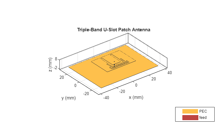
Modeling and Analysis of Single Layer Multi-Band U-Slot Patch Antenna
The standard rectangular microstrip patch is a narrowband antenna and provides 6-8 dBi Gain with linear polarization. This example is based on the work done in [1],[2], and models a broadband patch antenna using a slot in the radiator and develops a dual-band and a tri-band variation from it. In the process, the single wide response is split into multiple narrow band regions catering to specific bands in the WiMAX standard. These patch antennas are probe-fed.
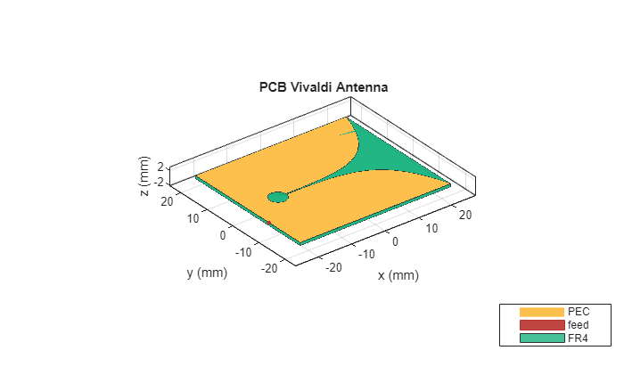
Design Internally Matched Ultra-Wideband Vivaldi Antenna
Model and analyze a vivaldi antenna with an internal matching circuit. The vivaldi is also known as an exponentially tapered slot antenna. The antenna possesses wideband characteristics, low cross polarization and a highly directive pattern. The design is implemented on a single layer dielectric substrate with 2 metal layers; one for a flared slot line, and the feed line with the matching circuit on the other layer. The substrate is chosen as a low cost FR4 material of thickness 0.8 mm. The design is intended for operation over the frequency band 3.1 - 10.6 GHz [1].
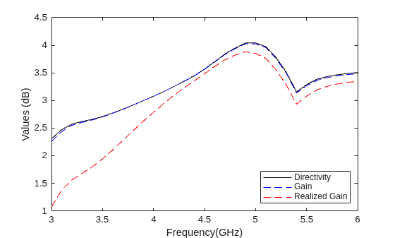
Design and Analysis of Compact Ultra-Wideband MIMO Antenna Array
Design and analysis of a compact ultra‑wideband MIMO antenna array operating from 3.1 to 10.6 GHz to address multipath fading and enhance channel capacity in UWB systems.
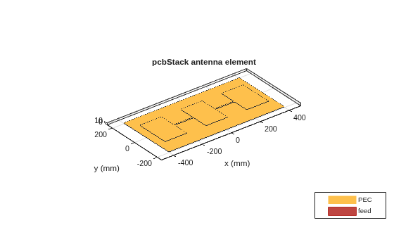
Design Variations of Microstrip Patch Antenna Using PCB Stack
Use the pcbstack to design basic, parasitic, direct-coupled, and CP patch antennas.
Model Coaxial Gap Feed for Probe-Fed Patch Antenna
Comparison of a standard delta-gap probe feed model and a finite-gap coaxial feed model for a patch antenna.

