Design, Analyze, and Prototype 2-by-2 Patch Antenna Array
This example shows how to create a 2-by-2 patch antenna array on an FR4 substrate, analyze the antenna, and generate PCB Gerber files for prototyping. The design operates at around 2.4 GHz.
Design Parameters
Set up the dielectric according to [1] and specify the physical constants.
freq = 2.4e9;
freqRange = linspace(2e9,3e9);
c = physconst("lightspeed");
d = dielectric("FR4");
d.EpsilonR = 4.3;
d.Thickness = 1.6e-3;
Calculate Patch Dimensions
Find the dimensions of the patch microstrip using the equations in [2]. The width and length are based on the effective permittivity and effective wavelength in the substrate.
W = c/(2*freq*sqrt((d.EpsilonR+1)/2));
epsilonEff = (d.EpsilonR+1)/2 + (d.EpsilonR-1)/2/sqrt(1+12*d.Thickness/W);
lambdaEff = c/(freq*sqrt(epsilonEff));
Leff = lambdaEff/2;
deltaL = 0.412*d.Thickness*(epsilonEff+0.3)*(W/d.Thickness+0.264)/(epsilonEff-0.258)/(W/d.Thickness+0.8);
L = Leff - 2*deltaL;
Create Patch
Create a square patch microstrip antenna element using the ground plane length and width described in [1].
GroundPlaneLength = 0.12;
GroundPlaneWidth = 0.12;
patch = patchMicrostrip(Substrate=d, Height=d.Thickness, Length=L, Width=L,...
    GroundPlaneLength=GroundPlaneLength/2, GroundPlaneWidth=GroundPlaneWidth/2,...
    FeedOffset=[0,0])
patch =
  patchMicrostrip with properties:

               Length: 0.0298
                Width: 0.0298
               Height: 0.0016
            Substrate: [1×1 dielectric]
    GroundPlaneLength: 0.0600
     GroundPlaneWidth: 0.0600
    PatchCenterOffset: [0 0]
           FeedOffset: [0 0]
            Conductor: [1×1 metal]
                 Tilt: 0
             TiltAxis: [1 0 0]
                 Load: [1×1 lumpedElement]
Create Array
Set the spacing between the elements in the array to be greater than half of the effective wavelength and create the rectangular array.
spacing = lambdaEff*0.6;
arr = rectangularArray(Element=patch,RowSpacing=spacing,ColumnSpacing=spacing)
arr =
  rectangularArray with properties:

           Element: [1×1 patchMicrostrip]
              Size: [2 2]
        RowSpacing: 0.0375
     ColumnSpacing: 0.0375
           Lattice: 'Rectangular'
    AmplitudeTaper: 1
        PhaseShift: 0
              Tilt: 0
          TiltAxis: [1 0 0]
arr.Element
ans =
  patchMicrostrip with properties:

               Length: 0.0298
                Width: 0.0298
               Height: 0.0016
            Substrate: [1×1 dielectric]
    GroundPlaneLength: 0.0600
     GroundPlaneWidth: 0.0600
    PatchCenterOffset: [0 0]
           FeedOffset: [0 0]
            Conductor: [1×1 metal]
                 Tilt: 0
             TiltAxis: [1 0 0]
                 Load: [1×1 lumpedElement]
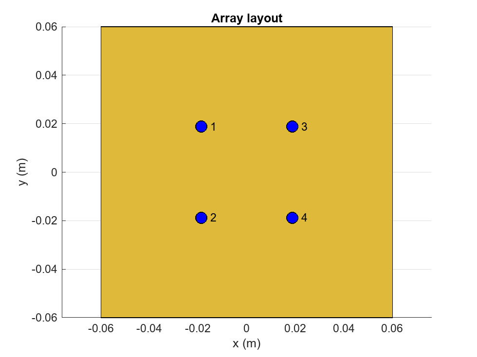
Display the layout and show the array without the traces. You can change this configuration so the bottom of the PCB has only one feed point.
layout(arr)
figure
title("Rectangular Array of Microstrip Patch Antenna");
show(arr)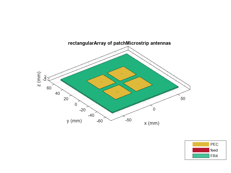
Create Feed Trace
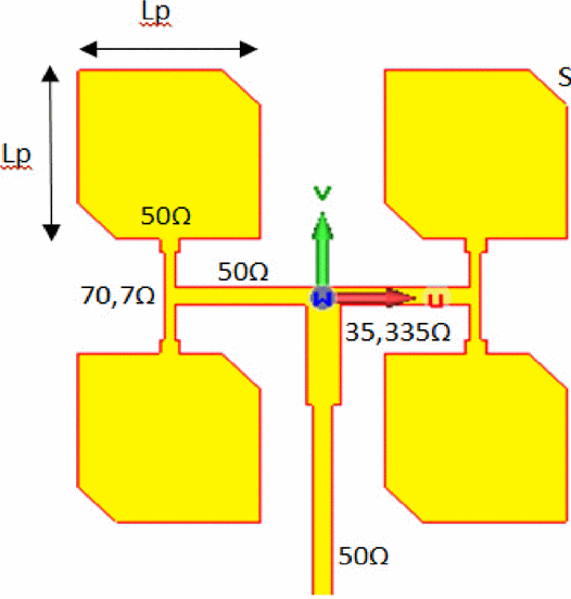
Create the trace from [1]. The authors use T-junction Wilkinson power dividers to impose a resistance of 50 at the feed points and at the edge of the patches. This figure from paper [1] shows the impedance of the traces.
z0 = 50;
traceWidth = traceThickness(z0,d)
traceWidth =
0.0031
z1 = real(z0)*sqrt(2);
traceWidth2 = traceThickness(z1,d)
traceWidth2 =
0.0017
z2 = real(z0)/sqrt(2);
traceWidth3 = traceThickness(z2,d)
traceWidth3 =
0.0053
offset = 3e-3;
feedLocation = -arr.GroundPlaneWidth/2 + offset;
x = abs(arr.FeedLocation(1,1));
y = abs(arr.FeedLocation(1,2));
firstTLength = 2*y;
secondTLength = 2*x + traceWidth2;
feedLength = traceWidth/2 - feedLocation;
feedTraceCenter = feedLocation + feedLength/2;
yLower = y - L/2;
patchFeedLength = L/2 + yLower/4;
patchFeedCenter = y - patchFeedLength/2;
feedTLength = feedLength/3;
feedTCenter = traceWidth/2 - feedTLength/2;
t1 = antenna.Rectangle(Length=traceWidth2,Width=firstTLength,Center=[x 0]);
t2 = antenna.Rectangle(Length=traceWidth2,Width=firstTLength,Center=[-x 0]);
t3 = antenna.Rectangle(Length=secondTLength,Width=traceWidth,Center=[0 0]);
t4 = antenna.Rectangle(Length=traceWidth,Width=feedLength,Center=[0 feedTraceCenter]);
t5 = antenna.Rectangle(Length=traceWidth,Width=patchFeedLength,Center=[x patchFeedCenter]);
t6 = antenna.Rectangle(Length=traceWidth,Width=patchFeedLength,Center=[-x patchFeedCenter]);
t7 = antenna.Rectangle(Length=traceWidth,Width=patchFeedLength,Center=[x -patchFeedCenter]);
t8 = antenna.Rectangle(Length=traceWidth,Width=patchFeedLength,Center=[-x -patchFeedCenter]);
t9 = antenna.Rectangle(Length=traceWidth3,Width=feedTLength,Center=[0 feedTCenter]);
feedTrace = t1 + t2 + t3 + t4 + t5 + t6 + t7 + t8 + t9;
figure(Name="Feed Trace")
show(feedTrace)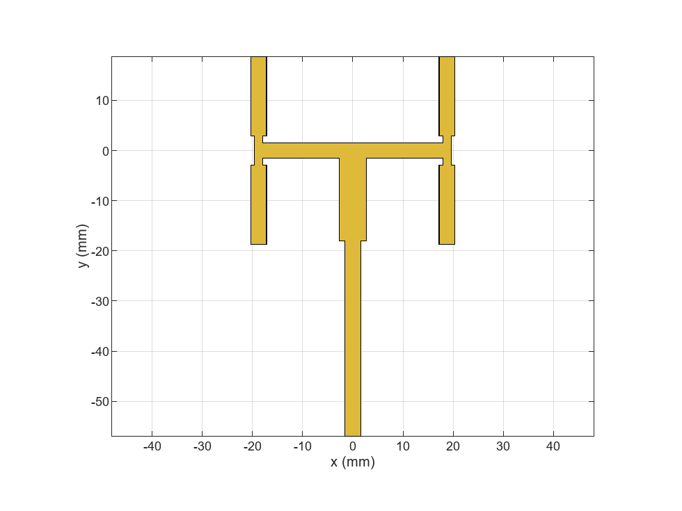
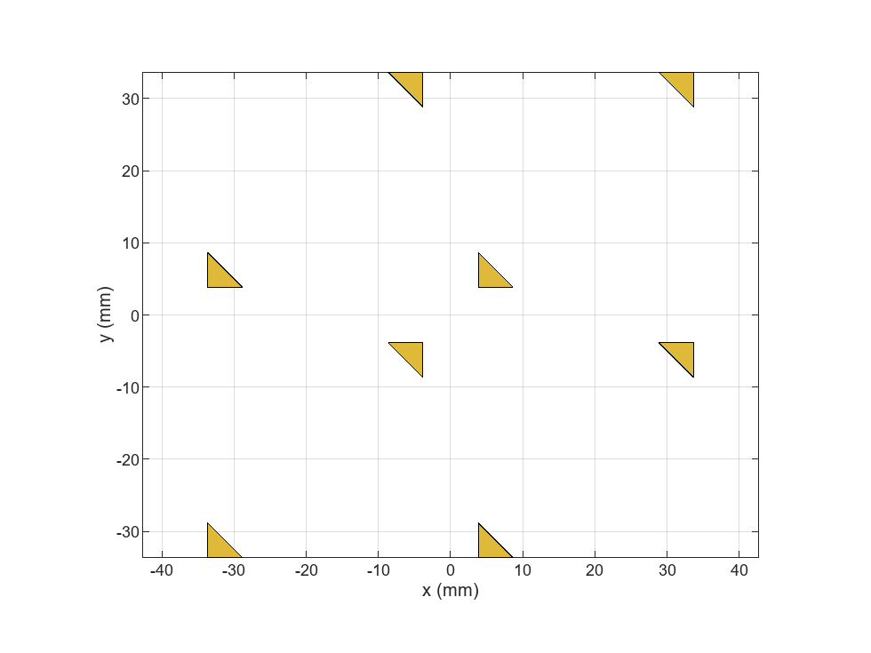
Sweep Side Lengths of Corners
Determine how much to cut off the corners by sweeping through possible side lengths of the triangle to cut and determine the impedance of the PCB. represents the ratio of triangle side length to the patch's length, so is the side length of the triangle that must be cut from the patch. Truncating the corners helps match the impedance to the desired value of 50 and the resonant frequency to 2.4 GHz.
The impedanceSweep MAT file contains a saved value of the impedance of a PCB with truncated corners whose side lengths are equal to . Because computing the impedance for all the different values of takes several hours, using the stored value in the MAT file speeds up the example. To calculate the value of z using the sweepImpedance function, set the calculateImpedance variable to true. The sweepImpedance function loops through values of to generate a PCB with truncated corners whose side lengths correspond to those values.
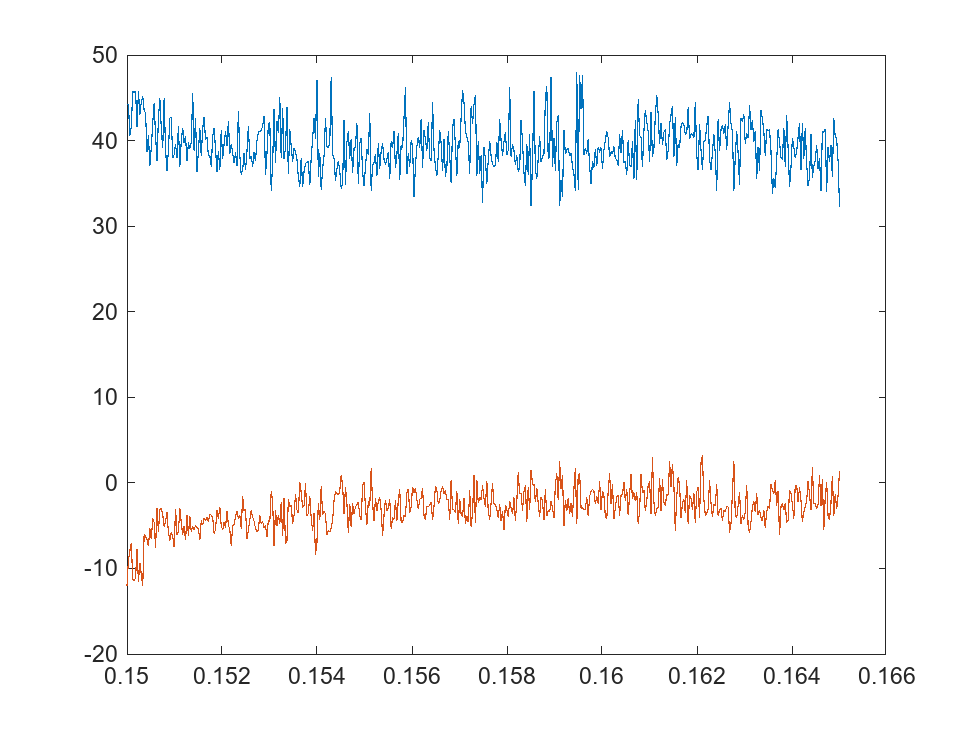
Plot the real and imaginary impedance as functions of .
S = linspace(0.15,0.165,500);
calculateImpedance = false;
if calculateImpedance
    z = sweepImpedance(arr,S,L,feedTrace,feedLocation,traceWidth,GroundPlaneLength,GroundPlaneWidth,freq);
else
    load("impedanceSweep.mat");
end
figure
plot(S,real(z))
hold on
plot(S,imag(z))
hold off
xlabel("Truncated Side Length");
ylabel("Impedance");
legend("Resistance","Reactance");
title("Impedance vs Truncated Side Length");
Create Truncated Corners
Find the value of that results in the PCB having impedance values closest to 50 resistance and 0 reactance. For this design, cut off isosceles right triangles with leg lengths equal to roughly 16% of the side length of a patch, or 4.7 mm.
[zmin,zidx] = min(abs(z-z0))
zmin =
1.9939
zidx =
425
z(zidx)
ans =
48.0072 + 0.0645i
S(zidx)
ans =
0.1627
s = S(zidx)*L
s =
0.0048
truncatedCorners = createTruncatedCorners(arr,s);
show(truncatedCorners)
Create PCB Stack Without Truncated Corners
Convert the array to a PCB stack and join the feed trace with the array. Then, set the feed and via locations and properties. Ensure that the PCB dielectric is as big as the ground plane.
arrPCB = pcbStack(arr);
arrPCB.Layers{1,1} = arrPCB.Layers{1,1} + feedTrace;
arrPCB.FeedLocations = [0 feedLocation 1 3];
arrPCB.ViaLocations = arrPCB.FeedLocations(1,:);
arrPCB.FeedDiameter = traceWidth/2;
arrPCB.ViaDiameter = arrPCB.FeedDiameter;
arrPCB.Layers{1,2}.Length = GroundPlaneLength;
arrPCB.Layers{1,2}.Width = GroundPlaneWidth;
figure
title("PCB Antenna")
show(arrPCB)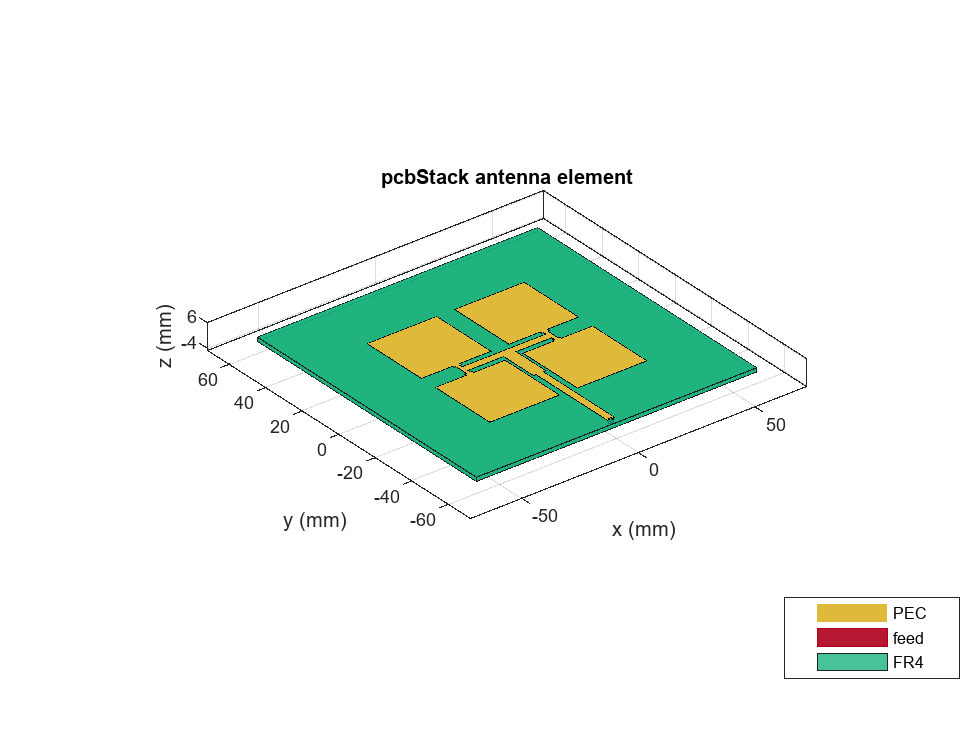
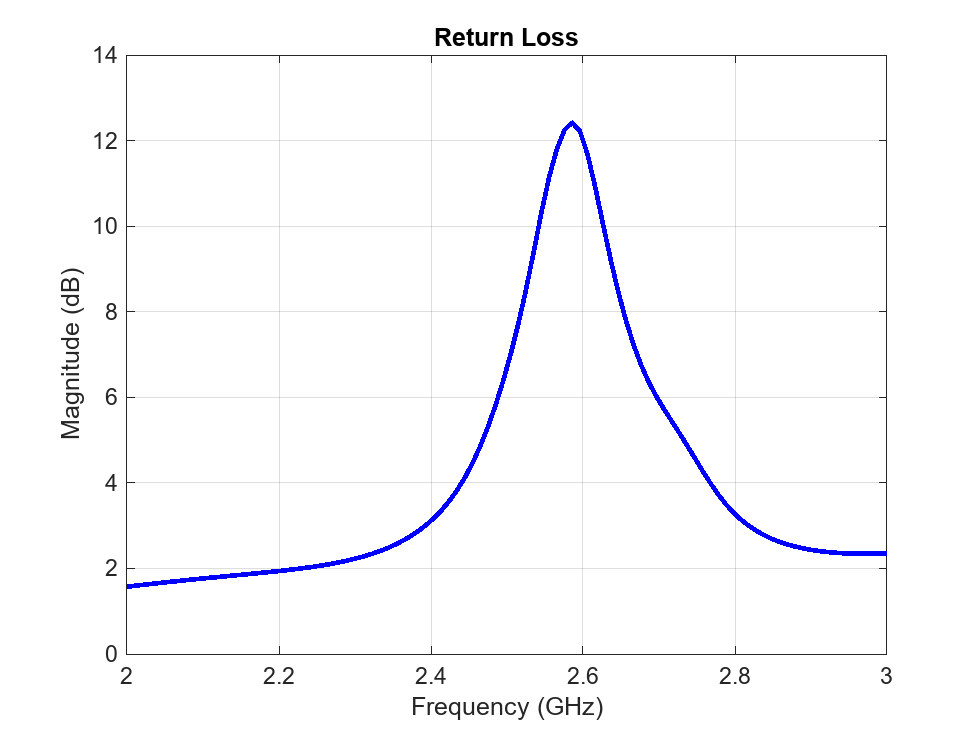
Analyze PCB Stack Without Truncated Corners
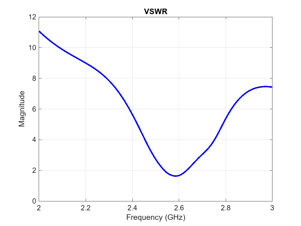
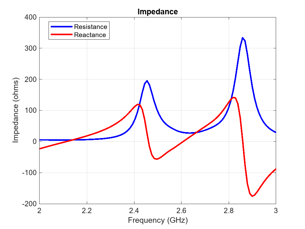
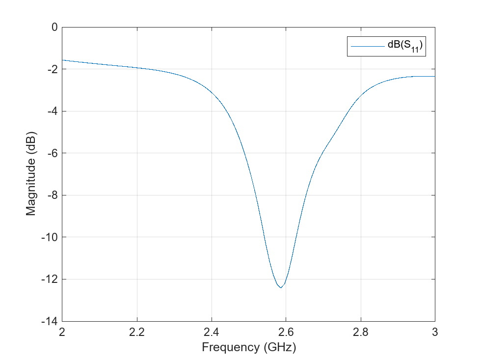
Analyze the PCB stack of the array that does not have truncated corners. Determine the return loss, the voltage standing wave ratio, the impedance, and the S-parameters.
returnLoss(arrPCB,freqRange,z0);
vswr(arrPCB,freqRange,z0);
impedance(arrPCB,freqRange);
spar = sparameters(arrPCB,freqRange,z0);
rfplot(spar)
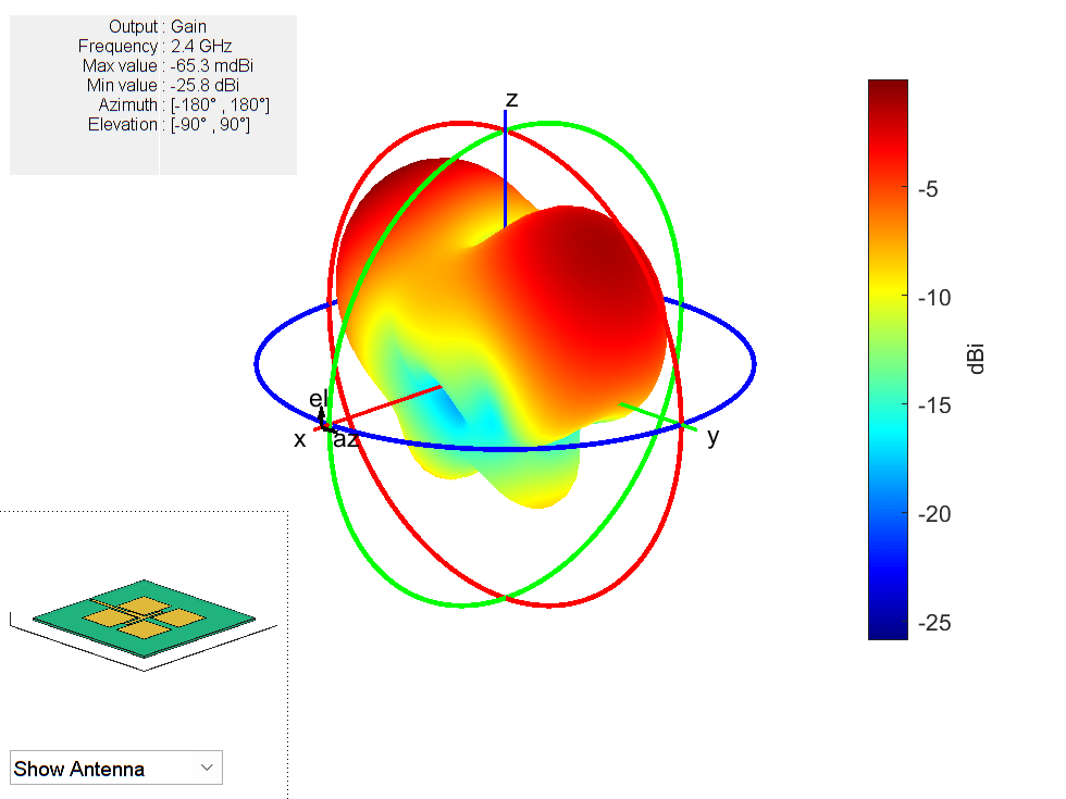
Show the PCB radiation pattern at 2.4 GHz.
pattern(arrPCB,freq)
Create PCB Stack with Truncated Corners
Convert the array to a PCB stack and join the feed trace with the array. Truncate the corners from the patches. Then, set the feed and via locations and properties. Ensure that the PCB dielectric substrate has same dimensions as the ground plane.
arrPCB_tc = pcbStack(arr);
arrPCB_tc.Layers{1,1} = arrPCB_tc.Layers{1,1} + feedTrace - truncatedCorners;
arrPCB_tc.FeedLocations = [0 feedLocation 1 3];
arrPCB_tc.ViaLocations = arrPCB_tc.FeedLocations(1,:);
arrPCB_tc.FeedDiameter = traceWidth/2;
arrPCB_tc.ViaDiameter = arrPCB_tc.FeedDiameter;
arrPCB_tc.Layers{1,2}.Length = GroundPlaneLength;
arrPCB_tc.Layers{1,2}.Width = GroundPlaneWidth;
figure
title("PCB Antenna with Truncated Corners")
show(arrPCB_tc)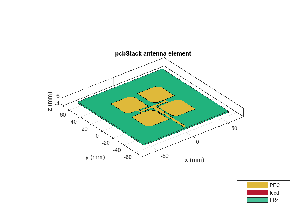
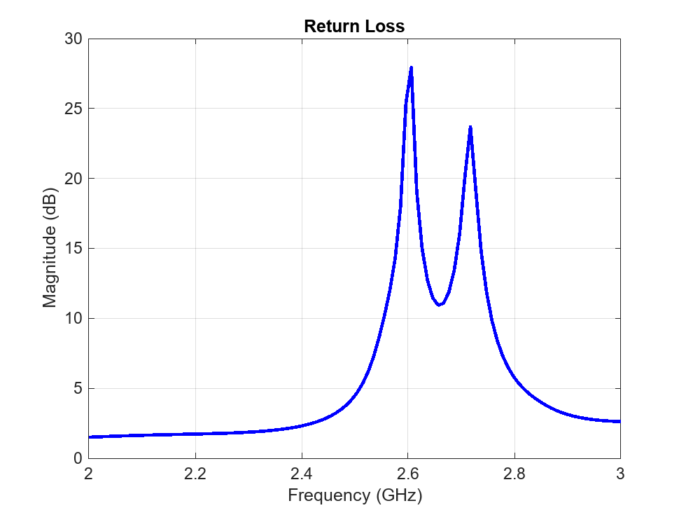
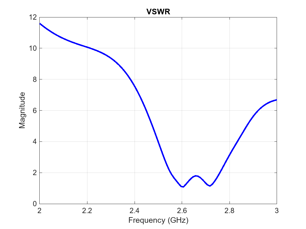
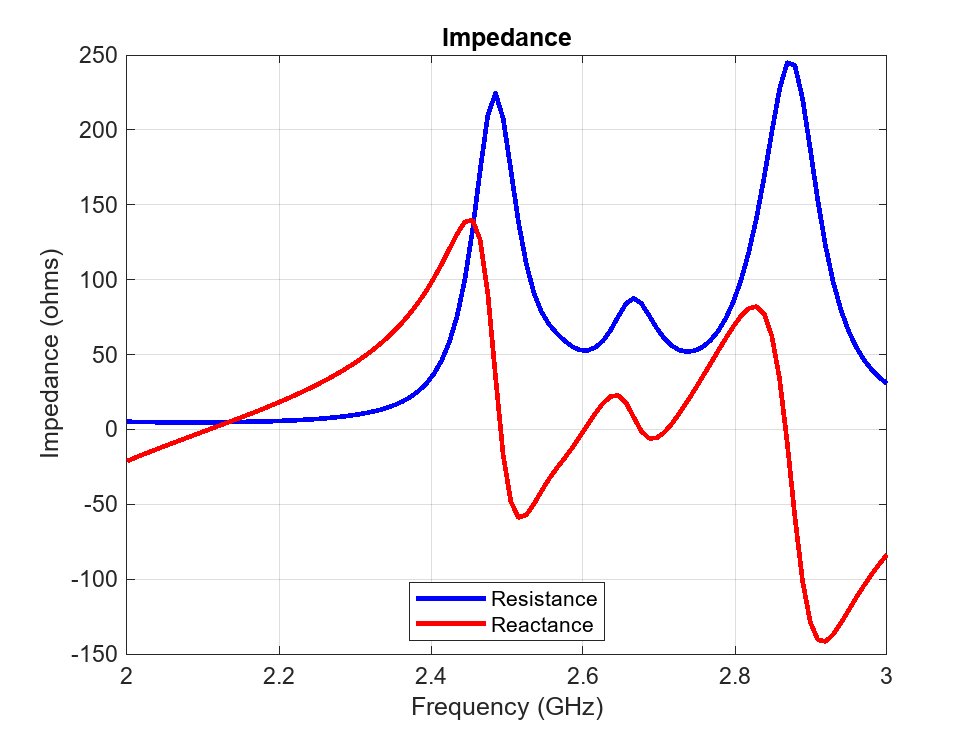
Analyze PCB Stack with Truncated Corners
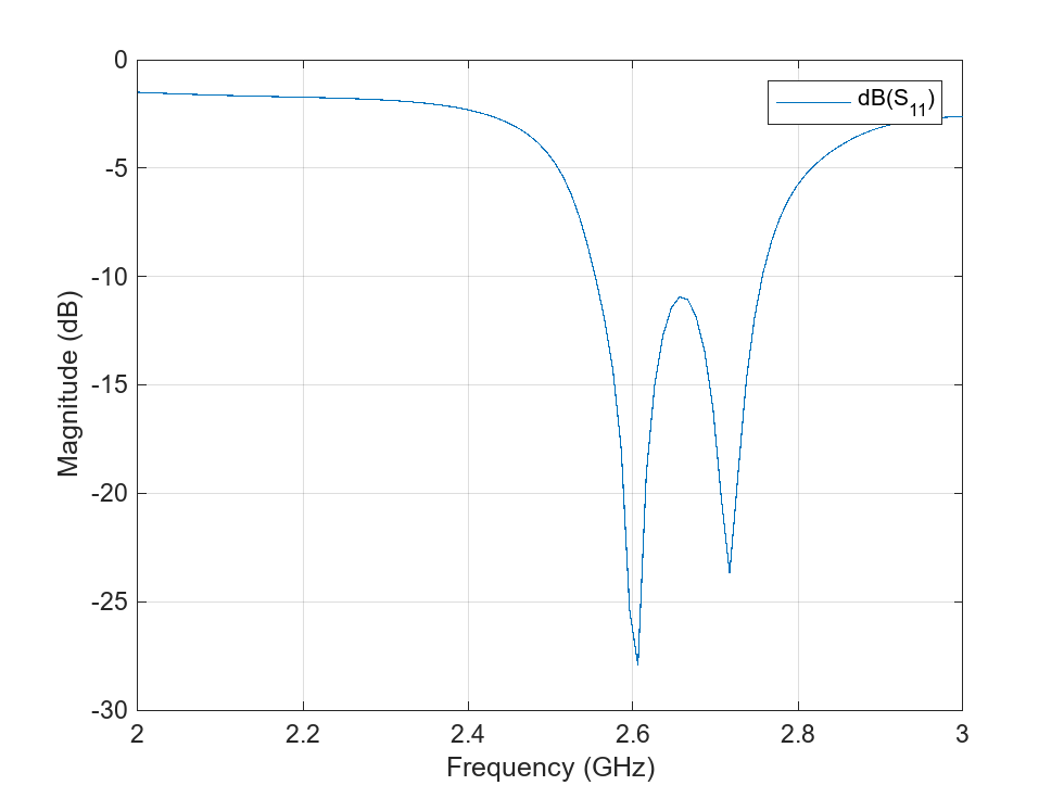
Analyze the PCB stack of the array with truncated corners. Determine the return loss, the voltage standing wave ratio, the impedance, and the S-parameters.
returnLoss(arrPCB_tc,freqRange,z0);
vswr(arrPCB_tc,freqRange,z0);
impedance(arrPCB_tc,freqRange);
spar = sparameters(arrPCB_tc,freqRange,z0);
rfplot(spar)
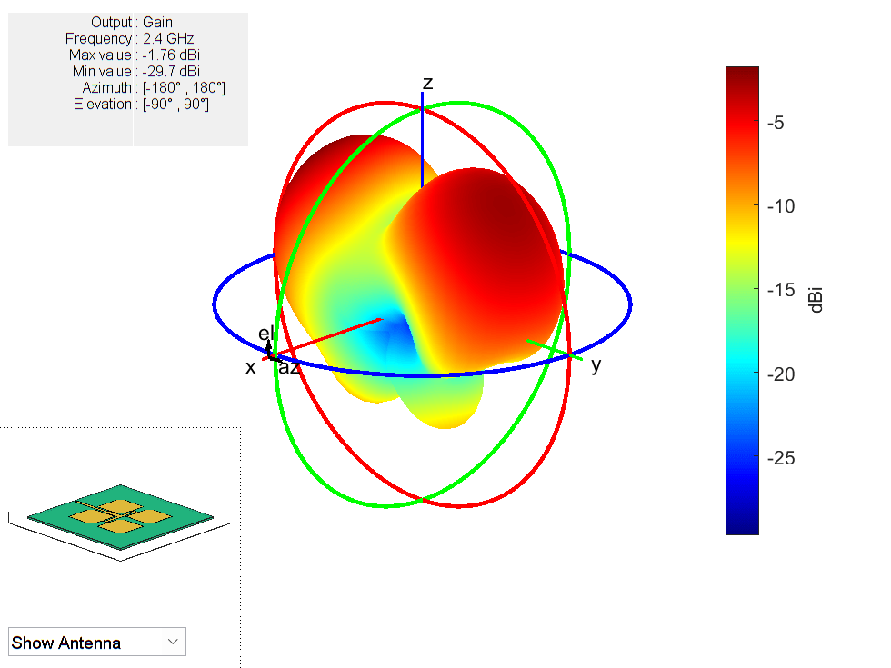
Show the PCB radiation pattern at 2.4 GHz.
pattern(arrPCB_tc,freq)
Generate Gerber Files
You can use Gerber files to export the geometry information of a PCB. Use a PCB writer and an RF connector to generate the Gerber files.
W = PCBServices.OSHParkWriter;
W = PCBServices.MayhewWriter;
W.Filename = 'patch array 2x2';
C = SMAEdge_SamtecCustom;
C.EdgeLocation = "south";
C.ExtendBoardProfile = false;
Am = PCBWriter(arrPCB_tc,W,C);
gerberWrite(Am)
If you have an internet connection, a browser window opens and displays the Mayhewlabs free 3D online Gerber viewer. After you drag and drop the files into the Mayhewslabs viewer, the software renders the PCB design. This figure shows the front view of the board.

This figure shows the back view of the board.

Conclusion
This example showed how to create a 2-by-2 patch antenna array with FR4 substrate, analyze the antenna array, and generate Gerber files of the PCB for prototyping.
Without truncated corners, the array has a single resonant frequency at 2.38 GHz. The reactance reaches 0 at around 2.45 GHz.
With the truncated corners, the array as multiple frequencies with dB in the S-parameter plot, one minimum at 2.39 GHz, and another minimum at 2.48 GHz. The reactance reaches 0 at around 2.41 GHz.
Supporting Functions
Determine Trace Widths
The traceThickness function determines the thickness of the traces on the PCB for input impedance and dielectric based on the equation from [1].
function width = traceThickness(z,d)
    A = z/60*sqrt((d.EpsilonR+1)/2)+(d.EpsilonR-1)/(d.EpsilonR+1)*(0.23+0.11/d.EpsilonR);
    width = d.Thickness*8*exp(A)/(exp(2*A)-2);
end
Create the Truncated Corners
The truncatedCorners function creates the truncated corners for the input array and leg length of an isosceles right triangle.
function truncatedCorners = createTruncatedCorners(arr,s)
    x11 = -arr.ColumnSpacing/2 + arr.Element.Length/2;
    y11 = arr.RowSpacing/2 + arr.Element.Width/2;
    x12 = -arr.ColumnSpacing/2 - arr.Element.Length/2;
    y12 = arr.RowSpacing/2 - arr.Element.Width/2;
    s1 = antenna.Polygon(Vertices=[x11-s y11 0; x11 y11-s 0; x11 y11 0]);
    s2 = antenna.Polygon(Vertices=[x12+s y12 0; x12 y12+s 0; x12 y12 0]);

    x21 = x11;
    y21 = -arr.RowSpacing/2+arr.Element.Width/2;
    x22 = x12;
    y22 = -arr.RowSpacing/2-arr.Element.Width/2;
    s3 = antenna.Polygon(Vertices=[x21-s y21 0; x21 y21-s 0; x21 y21 0]);
    s4 = antenna.Polygon(Vertices=[x22+s y22 0; x22 y22+s 0; x22 y22 0]);

    x31 = arr.ColumnSpacing/2 + arr.Element.Length/2;
    y31 = y11;
    x32 = arr.ColumnSpacing/2 - arr.Element.Length/2;
    y32 = y12;
    s5 = antenna.Polygon(Vertices=[x31-s y31 0; x31 y31-s 0; x31 y31 0]);
    s6 = antenna.Polygon(Vertices=[x32+s y32 0; x32 y32+s 0; x32 y32 0]);

    x41 = x31;
    y41 = y21;
    x42 = x32;
    y42 = y22;
    s7 = antenna.Polygon(Vertices=[x41-s y41 0; x41 y41-s 0; x41 y41 0]);
    s8 = antenna.Polygon(Vertices=[x42+s y42 0; x42 y42+s 0; x42 y42 0]);

    truncatedCorners = s1 + s2 + s3 + s4 + s5 + s6 + s7 + s8;
end
Calculate Impedance
For each element of the ratio S of truncated corner side length to patch length, the sweepImpedance function creates the truncated corners. The function then creates the PCB stack of the array, adds the feed trace, and removes the corners. You specify the feed and via locations and properties, ensuring that the PCB dielectric substrate has same dimensions as the ground plane. Finally, the function computes the impedance of the PCB.
function z = sweepImpedance(arr,S,L,feedTrace,feedLocation,traceWidth,GroundPlaneLength,GroundPlaneWidth,freq)
    z = zeros(size(S));
    for i = 1:length(S)
        s = S(i)*L;
        truncatedCorners = createTruncatedCorners(arr,s);

        pcb = pcbStack(arr);
        pcb.Layers{1,1} = pcb.Layers{1,1} + feedTrace - truncatedCorners;
        pcb.FeedLocations = [0 feedLocation 1 3];
        pcb.ViaLocations = pcb.FeedLocations(1,:);
        pcb.FeedDiameter = traceWidth/2;
        pcb.ViaDiameter = pcb.FeedDiameter;
        pcb.Layers{1,2}.Length = GroundPlaneLength;
        pcb.Layers{1,2}.Width = GroundPlaneWidth;
        % manually mesh the antenna
        mesh(pcb,'MaxEdgeLength',1.2*traceWidth)
        z(i) = impedance(pcb,freq);
        mesh(pcb);
    end
end
Reference
[1] Muludi, Zainal, and Budi Aswoyo. “Truncated Microstrip Square Patch Array Antenna 2 × 2 Elements with Circular Polarization for S-Band Microwave Frequency.” In 2017 International Electronics Symposium on Engineering Technology and Applications (IES-ETA), 87–92. Surabaya: IEEE, 2017. https://doi.org/10.1109/ELECSYM.2017.8240384.
[2] Balanis, Constantine A. Antenna Theory: Analysis and Design. Fourth edition. Hoboken, New Jersey: Wiley, 2016.
Copyright 2023 The MathWorks, Inc.