Half-Bridge (Ideal, Switching)

Libraries:
Simscape /
Electrical /
Semiconductors & Converters
Description
The Half-Bridge (Ideal, Switching) block models a half-bridge
with ideal switches and a thermal port. To choose the ideal switching device, set the
Switching device parameter to
MOSFET, IGBT, or
GTO.
You can specify an integral protection diode for each switching device. An integral diode protects the semiconductor device by providing a conduction path for a reverse current. An inductive load can produce a high reverse-voltage spike when the semiconductor device suddenly switches off the voltage supply to the load.
Note
The best option is to model diodes internally within the Half-Bridge (Ideal, Switching) block. To model the diodes externally, model them without capacitance or charge.
Switching Losses
For information about how the block models turn-on and turn-off losses, see the
documentation page for the MOSFET (Ideal, Switching) block, IGBT (Ideal, Switching) block, or GTO block, depending on the option you select for the
Switching Device parameter. The main difference between how
these blocks and the Half-Bridge (Ideal, Switching)
block model the losses is that, for the MOSFET and
IGBT options, the Half-Bridge (Ideal,
Switching) block does not use the Use last on-state
current from previous cycle for turn-on loss or Use last
off-state voltage from previous cycle for turn-off loss parameters.
The reason for this difference is that the Half-Bridge (Ideal,
Switching) block does not model diode capacitance or lead
inductance because the block is designed for fast simulation using ideal switching.
By modeling both switching devices in one block, you avoid the complexities
associated with measuring the on-state current and off-state voltage for diode
reverse recovery, so you do not need a physics-based diode charge model. The block
measures the diode forward current and off-state voltages at the point that you
command the complementary switching device to switch off.
By default, the block applies switching losses to the thermal node only, stepping the node temperature up by the requisite value. To draw the requisite power due to switching losses from the electrical supply, select the Apply switching losses to electrical supply parameter.
Instantaneously applying a switching loss to the electrical supply is not mathematically possible, so the block applies switching losses over a period equal to the value you specify for the Averaging period for switching losses parameter. Set this value equal to the pulse-width modulation (PWM) period of the gate driver.
Note
For all ideal switching devices, the logged simulation data reports the
thermal losses as lastTurnOffLoss,
lastTurnOnLoss, and
lastReverseRecoveryLoss. These variables include losses
as a pulse with an amplitude equal to the energy loss. If you use a script to
sum the total losses over a defined simulation period, you must sum the pulse
values at each pulse rising edge. Alternatively, you can extract conduction and
switching losses from logged data using the ee_getPowerLossSummary and
ee_getPowerLossTimeSeries functions.
To learn how to log and plot simulation data, see the Log and Plot Simulation Data example.
You can also access the total accumulated switching losses for each of the two
switching devices from the respective
accumulatedSwitchingLosses variables in the logged
simulation data. These variables sum all switching losses to date, including
reverse recovery losses for the diode.
The power_dissipated variable in the logged simulation data
does not include switching losses because the block models these losses as
instantaneous events. The power_dissipated variable reports
ohmic on-state losses.
If you are using a fixed-step solver, the shortest pulse on or pulse off that supports capture of the switching losses is three time steps long. If the pulse is shorter than three steps, the block does not report switching losses.
If you use tabulated data to model the switching losses or reverse recovery losses, check that the temperature, current, and voltage are in the range you specify. If you do not define a realistic thermal model, for example, if the junction mass or the conductance from the junction to the case is too small, the temperature can exceed the range you specify, causing the block to extrapolate the losses to nonphysical values.
Parameterization
The Half-Bridge (Ideal, Switching) block supports multiple predefined parameterizations.
Use this parameterization data to represent components by specific suppliers. The parameterizations of these half-bridges match the manufacturer data sheets. To load a predefined parameterization, double-click the Half-Bridge (Ideal, Switching) block, click the <click to select> hyperlink of the Selected part parameter, and, in the Block Parameterization Manager window, select the part you want to use from the list of available components.
Note
The predefined parameterizations of Simscape™ components use available data sources for the parameter values. Engineering judgment and simplifying assumptions are used to fill in for missing data. As a result, expect deviations between simulated and actual physical behavior. To ensure accuracy, validate the simulated behavior against experimental data and refine component models as necessary.
For more information about predefined parameterization and a list of the available components, see Simscape Electrical Part Collection.
You can also use the ee_importDeviceParameters function to extract the device parameters
for the switching device and integral protection diode from XML files and import
them into the block. The XML file must be on the MATLAB® path and must use a parameterization format supported by Hitachi or
Infineon®.
Thermal Port
Use the thermal port to simulate the effects of generated heat and device temperature. For more information on using thermal ports and the Thermal Port parameters, see Simulating Thermal Effects in Semiconductors.
You can also separate the thermal port H into two different thermal ports associated with the upper and lower switching devices, respectively, by selecting the Separate thermal ports for upper and lower devices parameter. If you separate the thermal ports for the upper and lower devices, you can then also separate the thermal ports for the integral diodes of each switching device by selecting the Separate thermal ports for integral diodes parameter. The upper and lower switching devices share the same thermal parameters. (since R2024a)
This figure shows the block icon when you expose all the thermal ports:

Variables
To set the priority and initial target values for the block variables before simulation, use the Initial Targets section in the block dialog box or Property Inspector. For more information, see Set Priority and Initial Target for Block Variables.
Use nominal values to specify the expected magnitude of a variable in a model. Using system scaling based on nominal values increases the simulation robustness. Nominal values can come from different sources. One of these sources is the Nominal Values section in the block dialog box or Property Inspector. For more information, see System Scaling by Nominal Values.
Examples
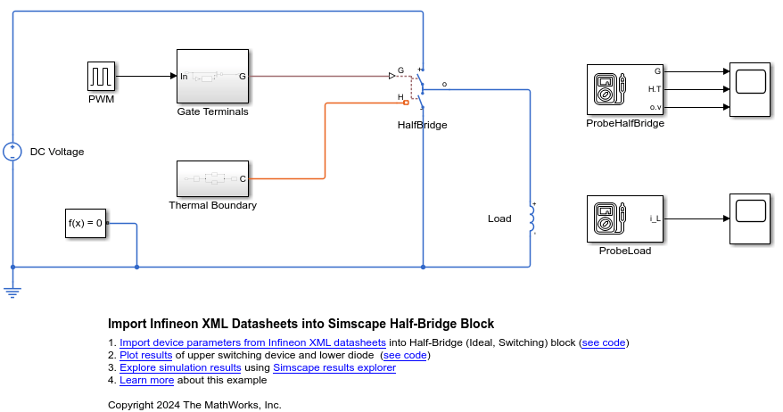
Import Infineon XML Datasheets into Simscape Half-Bridge Block
Import device parameters from Infineon® datasheets for IGBTs and diodes into a Half-Bridge (Ideal, Switching) block.
- Since R2024b
- Open Live Script
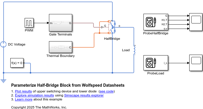
Parameterize Half-Bridge Block from Wolfspeed Datasheets
Import the device parameters from Wolfspeed® datasheets for MOSFETs and diodes into a Half-Bridge (Ideal, Switching) block.
- Since R2026a
- Open Live Script
Limitations
If you set the Switching device parameter to
GTO, the block assumes that the current change in the load between PWM cycles is small. This assumption implies that the load inductance or the switching frequency is large enough to smooth the current.If you select the Apply switching losses to electrical supply parameter, you must connect a power supply to the half-bridge. For example, you must clear the Apply switching losses to electrical supply parameter if your model has a switch that can disconnect one or both of the power supply connections. You can also encounter numerical initialization issues if the power supply does not initialize in the on state, for example, because of a smoothing capacitor that starts at zero charge.
Ports
Input
Physical signal conserving port associated with the gate terminals of the two switching devices, specified as a vector of two physical signals.
The first element of the vector controls the upper side switch. The
second element of the vector controls the lower side switch. If, in the
Diode settings, you set the Integral
protection diode parameter to
Yes, the first and second element of the
vector also controls the lower and upper diode, respectively.
Dependencies
To enable this port, set Gate-control port to
PS.
Conserving
Electrical conserving port associated with the positive terminal.
Electrical conserving port associated with the negative terminal.
Electrical conserving port associated with the output node.
Electrical conserving port associated with the gate terminal for the first switching device.
Dependencies
To enable this port, set Gate-control port to
Electrical.
Electrical conserving port associated with the gate terminal for the second switching device.
Dependencies
To enable this port, set Gate-control port to
Electrical.
Thermal conserving port.
Dependencies
To enable this port, clear the Separate thermal ports for upper and lower devices and Separate thermal ports for integral diodes parameters.
Since R2024a
Thermal conserving port associated with the upper switching device.
Dependencies
To enable this port, select the Separate thermal ports for upper and lower devices parameter.
Since R2024a
Thermal conserving port associated with the lower switching device.
Dependencies
To enable this port, select the Separate thermal ports for upper and lower devices parameter.
Since R2024a
Thermal conserving port associated with the upper diode.
Dependencies
To enable this port, select the Separate thermal ports for upper and lower devices and Separate thermal ports for integral diodes parameters.
Since R2024a
Thermal conserving port associated with the lower diode.
Dependencies
To enable this port, select the Separate thermal ports for upper and lower devices and Separate thermal ports for integral diodes parameters.
Parameters
Part Repository
Use the Select part button to open the Block Parameterization Manager tool and view the available parts.
Active part associated with the block.
Dependencies
To enable this parameter, apply a part to the block by using the Block Parameterization Manager.
Click the Restore parameters button to restore the parameterization to the active part. The name of the parameter is Status: unmodified if the part uses the default properties for the parameter, and Status: modified if the parameters have been modified from the associated active part.
Dependencies
To enable this parameter, apply a part to the block by using the Block Parameterization Manager.
Use the Clear part association button to clear the active part associated with the block.
Dependencies
To enable this parameter, apply a part to the block by using the Block Parameterization Manager.
Main
The visibility of the Main parameters depends on the Switching device and On-state behavior and losses parameters. To learn how to read this table, see Parameter Dependencies.
Main Parameter Dependencies
| Parameters and Options | |||||
|---|---|---|---|---|---|
| Gate-control port | |||||
| Switching Device | |||||
MOSFET | IGBT | GTO | |||
| Threshold voltage, Vth | Threshold voltage, Vth | Gate trigger voltage, Vgt | |||
| Gate turn-off voltage, Vgt_off | |||||
| Holding current | |||||
| On-state behavior and losses | On-state behavior and losses | On-state behavior and losses | |||
Specify constant
values | Tabulate | Specify constant
values | Tabulate | Specify constant
values | Tabulate |
| Drain-source on resistance, R_DS(on) | On-state voltage, Vds(Tj,Ids) | Forward voltage, Vf | On-state voltage, Vds(Tj,Ice) | Forward voltage, Vf | On-state voltage, Vak(Tj,Iak) |
| Temperature vector, Tj | On-state resistance | Temperature vector, Tj | On-state resistance | Temperature vector, Tj | |
| Drain-source current vector, Ids | Collector-emitter current vector, Ice | Anode-cathode current vector, Iak | |||
| Off-state conductance | |||||
Option to use the physical signal input port G or the electrical conserving ports G1 and G2 as the gate control ports.
Switching device for the half-bridge.
Threshold voltage at which the device turns on. The default value depends on the Switching device setting.
Dependencies
See the Main Parameter Dependencies table.
Gate-cathode voltage threshold. The device turns on when the gate-cathode voltage is above this value.
Dependencies
See the Main Parameter Dependencies table.
Gate-cathode voltage threshold. The device turns off when the gate-cathode voltage is below this value.
Dependencies
See the Main Parameter Dependencies table.
Current threshold. The device stays on when the current is above this value, even when the gate-cathode voltage falls below the gate trigger voltage.
Dependencies
See the Main Parameter Dependencies table.
Parameterization method for on-state behavior and switching losses, specified as one of these values:
Specify constant values— Use scalar values to specify the output current, switch-on loss, and switch-off loss data. The block assumes that the energy dissipated during a single switch-on or switch-off event scales linearly with the off-state voltage and on-state current. The block also assumes that the losses are independent of temperature.Tabulate— Use vectors to specify the output current and temperature data. Use arrays to specify the switch-on loss and switch-off loss data.
Dependencies
See the Main Parameter Dependencies table.
Drain-source resistance when the device is on.
Dependencies
See the Main Parameter Dependencies table.
Voltage drop across the device in a triggered conductive state. This parameter is a function of temperature and final on-state output current.
Dependencies
See the Main Parameter Dependencies table.
Drain-source currents at which you quote the on-state voltage. The sign of the drain-source current must be the same as the sign of the corresponding drain-source voltage. If the drain-source voltage is zero, the corresponding drain-source current must also be zero.
Dependencies
See the Main Parameter Dependencies table.
Minimum voltage required across the collector and emitter or anode and cathode block ports for the gradient of the diode I-V characteristic to be 1/Ron, where Ron is the value of the On-state resistance parameter.
Dependencies
See the Main Parameter Dependencies table.
Collector-emitter resistance when the device is on.
Dependencies
See the Main Parameter Dependencies table.
Voltage drop across the device in a triggered conductive state. This parameter is a function of temperature and final on-state output current.
Dependencies
See the Main Parameter Dependencies table.
Collector-emitter currents at which you quote the on-state voltage. The sign of the collector-emitter current must be the same as the sign of the corresponding collector-emitter voltage. If the collector-emitter voltage is zero, the corresponding collector-emitter current must also be zero.
Dependencies
See the Main Parameter Dependencies table.
Voltage drop across the device in a triggered conductive state. This parameter is a function of temperature and final on-state output current.
Dependencies
See the Main Parameter Dependencies table.
Anode-cathode currents at which you quote the on-state voltage. The sign of the anode-cathode current must be the same as the sign of the corresponding anode-cathode voltage. If the anode-cathode voltage is zero, the corresponding anode-cathode current must also be zero.
Dependencies
See the Main Parameter Dependencies table.
Temperature values at which you quote the on-state voltage.
Dependencies
See the Main Parameter Dependencies table.
Conductance when the device is off. The value must be less than 1/R, where R is the value of the On-state resistance parameter.
Dependencies
See the Main Parameter Dependencies table.
Losses
Energy dissipated during a single switch-on event.
Dependencies
To enable this parameter, set On-state behavior and
losses to Specify constant
values.
Energy dissipated during a single switch-off event.
Dependencies
To enable this parameter, set Switching
device to MOSFET or
IGBT and set On-state
behavior and losses to Specify constant
values.
Energy dissipated during a diode-reverse recovery event.
Dependencies
To enable this parameter, set On-state behavior and
losses to Specify constant
values and set Integral protection
diode to Yes.
Output current at which you quote the switch-on loss, switch-off loss, and on-state voltage.
Dependencies
To enable this parameter, set On-state behavior and
losses to Specify constant
values.
Output voltage when the device is off. This value is the blocking
voltage at which you quote the losses. If you specify switching losses
as scalar values or as a function of the junction temperature and
on-state current at a fixed off-state voltage, the block uses this value
to calculate switching losses. If you set Integral protection
diode to Yes, the block uses
this value to calculate diode reverse recovery loss.
Dependencies
To enable this parameter, choose one of these options:
Set On-state behavior and losses to
Specify constant values.Set Switching device to
MOSFET, set On-state behavior and losses toTabulate, and clear the Use separate axes for switching losses and reverse recovery loss parameter. (since R2026a)Set Switching device to
IGBT, set On-state behavior and losses toTabulate, and clear the Use separate axes for switching losses and reverse recovery loss parameter. (since R2026a)Set Switching device to
GTO.
Since R2026a
Option to specify separate temperature, current, and voltage axes values for tabulating switching and reverse recovery losses.
Clear this parameter to tabulate the switch-on loss, switch-off loss, and reverse recovery loss with the same values of temperature and current. If you select the Include switching loss tabulation with off-state Vds voltage or Include switching loss tabulation with off-state voltage, you can also include the off-state voltage in the tabulation for the switch-on and switch-off losses.
Select this parameter to tabulate the switch-on loss and switch-off loss with one set of temperature,current, and voltage values, and the reverse recovery loss with another set of different temperature, current, and voltage values. This is the only option that allows you to tabulate the reverse recovery loss with the off-state voltage.
Dependencies
To enable this parameter:
In the Main section, set On-state behavior and losses to
Tabulate.In the Integral Diode section, set Integral protection diode to
Yes.
Energy dissipated during a single switch-on event as a function of temperature and final on-state drain-source current.
Dependencies
To enable this parameter:
Set Switching device to
MOSFET.Set On-state behavior and losses to
Tabulate.Clear the Include switching loss tabulation with off-state Vds voltage parameter.
Clear the Use separate axes for switching losses and reverse recovery loss parameter. (since R2026a)
Energy dissipated during a single switch-off event as a function of temperature and final on-state drain-source current.
Dependencies
To enable this parameter:
Set Switching device to
MOSFET.Set On-state behavior and losses to
Tabulate.Clear the Include switching loss tabulation with off-state Vds voltage parameter.
Clear the Use separate axes for switching losses and reverse recovery loss parameter. (since R2026a)
Energy dissipated during a diode-reverse recovery event as a function of temperature and final on-state drain-source current.
Dependencies
To enable this parameter:
Set Switching device to
MOSFET.Set On-state behavior and losses to
Tabulate.Set Integral protection diode to
Yes.Clear the Use separate axes for switching losses and reverse recovery loss parameter. (since R2026a)
Temperature values at which you quote the losses.
Dependencies
To enable this parameter, set On-state behavior and
losses to Tabulate.
Drain-source currents at which you quote the losses. The sign of the drain-source current must be the same as the sign of the corresponding drain-source voltage. If the drain-source voltage is zero, the corresponding drain-source current must also be zero.
Dependencies
To enable this parameter, set Switching
device to MOSFET and set
On-state behavior and losses to
Tabulate.
Since R2023b
Off-state voltage at which you quote the losses.
Dependencies
To enable this parameter, set Switching
device to MOSFET and set
On-state behavior and losses to
Tabulate.
Then, select one of these condition sets:
Condition Set One
In the Integral Diode section, set the Integral protection diode parameter to
No.In the Losses section, select the Include switching loss tabulation with off-state Vds voltage parameter.
Condition Set Two
In the Integral Diode section, set the Integral protection diode parameter to
Yes.In the Losses section, select the Include switching loss tabulation with off-state Vds voltage parameter.
Condition Set Three
In the Integral Diode section, set the Integral protection diode parameter to
Yes.In the Losses section, select the Use separate axes for switching losses and reverse recovery loss parameter. (since R2026a)
Since R2023b
Option to tabulate the switching losses with the off-state drain-source voltage.
Clear this parameter to tabulate the switch-on loss and switch-off loss with the on-state drain-source current and temperature. The block assumes that the losses scale linearly with the off-state drain-source voltage.
Select this parameter to tabulate the switch-on loss and switch-off loss with the temperature, on-state drain-source current, and off-state drain-source voltage.
Dependencies
To enable this parameter:
Set Switching device to
MOSFET.Set On-state behavior and losses to
Tabulate.Clear the Use separate axes for switching losses and reverse recovery loss parameter. (since R2026a)
Since R2023b
Energy dissipated during a single switch-on event as a function of temperature, on-state drain-source current, and off-state drain-source voltage.
Dependencies
To enable this parameter, set these conditions:
In the Main section:
Set Switching device to
MOSFET.Set On-state behavior and losses to
Tabulate.
In the Losses section, choose one of these two options:
Select the Include switching loss tabulation with off-state Vds voltage parameter.
Select the Use separate axes for switching losses and reverse recovery loss parameter. (since R2026a)
Since R2023b
Energy dissipated during a single switch-off event as a function of temperature, on-state drain-source current, and off-state drain-source voltage.
Dependencies
To enable this parameter, set these conditions:
In the Main section:
Set Switching device to
MOSFET.Set On-state behavior and losses to
Tabulate.
In the Losses section, choose one of these two options:
Select the Include switching loss tabulation with off-state Vds voltage parameter.
Select the Use separate axes for switching losses and reverse recovery loss parameter. (since R2026a)
Since R2026a
Dissipated energy as a function of the junction temperature Tj, drain-source current Ids just before the switching event, and turn-off voltage after the reverse recovery event Vds.
Dependencies
To enable this parameter:
In the Main section:
Set Switching device to
MOSFET.Set On-state behavior and losses to
Tabulate.
In the Integral Diode section, set Integral protection diode to
Yes.In the Losses section, select the Use separate axes for switching losses and reverse recovery loss parameter.
Since R2026a
Temperature vector that the block uses to tabulate the diode reverse recovery loss.
Dependencies
To enable this parameter:
In the Main section, set On-state behavior and losses to
Tabulate.In the Integral Diode section, set Integral protection diode to
Yes.In the Losses section, select the Use separate axes for switching losses and reverse recovery loss parameter.
Since R2026a
Drain-source currents at which you quote the diode reverse recovery losses. The sign of the drain-source current must be the same as the sign of the corresponding drain-source voltage. If the drain-source voltage is zero, the corresponding drain-source current must also be zero.
Dependencies
To enable this parameter:
In the Main section:
Set Switching device to
MOSFET.Set On-state behavior and losses to
Tabulate.
In the Integral Diode section, set Integral protection diode to
Yes.In the Losses section, select the Use separate axes for switching losses and reverse recovery loss parameter.
Since R2026a
Off-state voltages at which you quote the diode reverse recovery losses.
Dependencies
To enable this parameter:
In the Main section:
Set Switching device to
MOSFET.Set On-state behavior and losses to
Tabulate.
In the Integral Diode section, set Integral protection diode to
Yes.In the Losses section, select the Use separate axes for switching losses and reverse recovery loss parameter.
Since R2023b
Option to tabulate the switching losses with the off-state voltage.
Clear this parameter to tabulate the switch-on loss and switch-off loss with the on-state collector-emitter current and temperature. The block assumes that the losses scale linearly with the off-state voltage.
Select this parameter to tabulate the switch-on loss and switch-off loss with the temperature, on-state collector-emitter current, and off-state voltage.
Dependencies
To enable this parameter:
In the Main section:
Set Switching device to
IGBT.Set On-state behavior and losses to
Tabulate.
In the Losses section, select the Use separate axes for switching losses and reverse recovery loss parameter.
Energy dissipated during a single switch-on event as a function of temperature and final on-state collector-emitter current.
Dependencies
To enable this parameter:
Set Switching device to
IGBT.Set On-state behavior and losses to
Tabulate.Clear the Include switching loss tabulation with off-state voltage parameter.
Clear the Use separate axes for switching losses and reverse recovery loss parameter. (since R2026a)
Energy dissipated during a single switch-off event as a function of temperature and final on-state collector-emitter current.
Dependencies
To enable this parameter:
Set Switching device to
IGBT.Set On-state behavior and losses to
Tabulate.Clear the Include switching loss tabulation with off-state voltage parameter.
Clear the Use separate axes for switching losses and reverse recovery loss parameter. (since R2026a)
Energy dissipated during a diode-reverse recovery event as a function of temperature and final on-state collector-emitter current.
Dependencies
To enable this parameter:
Set Switching device to
IGBT.Set On-state behavior and losses to
Tabulate.Set Integral protection diode to
Yes.Clear the Use separate axes for switching losses and reverse recovery loss parameter. (since R2026a)
Collector-emitter currents at which you quote the losses. The sign of the collector-emitter current must be the same as the sign of the corresponding collector-emitter voltage. If the collector-emitter voltage is zero, the corresponding collector-emitter current must also be zero.
Dependencies
To enable this parameter, set Switching device to
IGBT and set On-state
behavior and losses to
Tabulate.
Since R2023b
Energy dissipated during a single switch-on event as a function of temperature, on-state collector-emitter current, and off-state collector-emitter voltage.
Dependencies
To enable this parameter, set these conditions:
In the Main section:
Set Switching device to
IGBT.Set On-state behavior and losses to
Tabulate.
In the Losses section, choose one of these two options:
Select the Include switching loss tabulation with off-state voltage parameter.
Select the Use separate axes for switching losses and reverse recovery loss parameter. (since R2026a)
Since R2023b
Energy dissipated during a single switch-off event as a function of temperature, on-state collector-emitter current, and off-state collector-emitter voltage.
Dependencies
To enable this parameter, set these conditions:
In the Main section:
Set Switching device to
IGBT.Set On-state behavior and losses to
Tabulate.
In the Losses section, choose one of these two options:
Select the Include switching loss tabulation with off-state voltage parameter.
Select the Use separate axes for switching losses and reverse recovery loss parameter. (since R2026a)
Since R2023b
Off-state collector-emitter voltages at which you quote the switch-on loss and switch-off loss.
Dependencies
To enable this parameter, set Switching
device to IGBT and set
On-state behavior and losses to
Tabulate.
Then, select one of these condition sets:
Condition Set One
In the Integral Diode section, set the Integral protection diode parameter to
No.In the Losses section, select the Include switching loss tabulation with off-state Vds voltage parameter.
Condition Set Two
In the Integral Diode section, set the Integral protection diode parameter to
Yes.In the Losses section, select the Include switching loss tabulation with off-state Vds voltage parameter.
Condition Set Three
In the Integral Diode section, set the Integral protection diode parameter to
Yes.In the Losses section, select the Use separate axes for switching losses and reverse recovery loss parameter.
Since R2026a
Dissipated energy as a function of the junction temperature Tj, collector-emitter current Ice just before the switching event, and turn-off voltage after the reverse recovery event Vce.
Dependencies
To enable this parameter:
In the Main section:
Set Switching device to
IGBT.Set On-state behavior and losses to
Tabulate.
In the Integral Diode section, set Integral protection diode to
Yes.In the Losses section, select the Use separate axes for switching losses and reverse recovery loss parameter.
Since R2026a
Collector-emitter currents at which you quote the diode reverse recovery losses. The sign of the collector-emitter must be the same as the sign of the corresponding collector-emitter voltage. If the collector-emitter voltage is zero, the corresponding collector-emitter current must also be zero.
Dependencies
To enable this parameter:
In the Main section:
Set Switching device to
IGBT.Set On-state behavior and losses to
Tabulate.
In the Integral Diode section, set Integral protection diode to
Yes.In the Losses section, select the Use separate axes for switching losses and reverse recovery loss parameter.
Since R2026a
Off-state voltages at which you quote the diode reverse recovery losses.
Dependencies
To enable this parameter:
In the Main section:
Set Switching device to
IGBT.Set On-state behavior and losses to
Tabulate.
In the Integral Diode section, set Integral protection diode to
Yes.In the Losses section, select the Use separate axes for switching losses and reverse recovery loss parameter.
Energy dissipated during a forced commutation switch-off event.
Dependencies
To enable this parameter, set Switching
device to GTO and set
On-state behavior and losses to
Specify constant values.
Rectification loss that the block applies when the device switches off because the current falls below the value of the Holding current parameter.
Dependencies
To enable this parameter, set Switching
device to GTO.
Energy dissipated during a single switch-on event as a function of temperature and final on-state anode-cathode current.
Dependencies
To enable this parameter:
In the Main section, set:
Switching device to
GTO.On-state behavior and losses to
Tabulate.
In the Losses section, clear the Use separate axes for switching losses and reverse recovery loss parameter. (since R2026a)
and.
Energy dissipated during a single switch-off event as function of temperature and final on-state anode-cathode current.
Dependencies
To enable this parameter:
In the Main section, set:
Switching device to
GTO.On-state behavior and losses to
Tabulate.
In the Losses section, clear the Use separate axes for switching losses and reverse recovery loss parameter. (since R2026a)
and.
Energy dissipated during a diode-reverse recovery event as a function of temperature and final on-state anode-cathode current.
Dependencies
To enable this parameter:
In the Main section, set:
Switching device to
GTO.On-state behavior and losses to
Tabulate.
In the Integral Diode section, set Integral protection diode to
Yes.In the Losses section, clear the Use separate axes for switching losses and reverse recovery loss parameter. (since R2026a)
Anode-cathode currents at which you quote the losses. The sign of the anode-cathode current must be the same as the sign of the corresponding anode-cathode voltage. If the anode-cathode voltage is zero, the corresponding anode-cathode current must also be zero.
Dependencies
To enable this parameter, set Switching
device to GTO and set
On-state behavior and losses to
Tabulate.
Since R2026a
Dissipated energy as a function of the junction temperature Tj, anode-cathode current Iak just before the switching event, and turn-off voltage after the reverse recovery event Vak.
Dependencies
To enable this parameter:
In the Main section:
Set Switching device to
GTO.Set On-state behavior and losses to
Tabulate.
In the Integral Diode section, set Integral protection diode to
Yes.In the Losses section, select the Use separate axes for switching losses and reverse recovery loss parameter.
Since R2026a
Anode-cathode currents at which you quote the diode reverse recovery losses. The sign of the anode-cathode current must be the same as the sign of the corresponding anode-cathode voltage. If the anode-cathode voltage is zero, the corresponding anode-cathode current must also be zero.
Dependencies
To enable this parameter:
In the Main section:
Set Switching device to
GTO.Set On-state behavior and losses to
Tabulate.
In the Integral Diode section, set Integral protection diode to
Yes.In the Losses section, select the Use separate axes for switching losses and reverse recovery loss parameter.
Since R2026a
Off-state voltages at which you quote the diode reverse recovery losses.
Dependencies
To enable this parameter:
In the Main section:
Set Switching device to
GTO.Set On-state behavior and losses to
Tabulate.
In the Integral Diode section, set Integral protection diode to
Yes.In the Losses section, select the Use separate axes for switching losses and reverse recovery loss parameter.
Since R2023b
Option to apply the switching losses to the electrical supply.
Clear this parameter to apply the switching losses to the thermal node only.
Select this parameter to apply the switching losses to the thermal node and the electrical supply.
Since R2023b
Duration over which the block applies the switching losses to the electrical supply.
Dependencies
To enable this parameter, select the Apply switching losses to electrical supply parameter.
Integral Diode
Whether to model the block integral protection diode.
Diode model, specified as either:
Piecewise Linear— Use a piecewise linear model for the diode, as described in Piecewise Linear Diode.Tabulated I-V curve— Use tabulated forward bias I-V data and fixed reverse bias off conductance.
Dependencies
To enable this parameter, set Integral protection
diode to Yes.
Minimum voltage required across the + and - block
ports for the gradient of the diode I-V characteristic to be
1/Ron, where
Ron is the value of the
On resistance parameter.
Dependencies
To enable this parameter, set Integral protection diode to
Yes and Diode
model to Piecewise linear.
Rate of change of the voltage versus the current above the value of the Forward voltage parameter.
Dependencies
To enable this parameter, set Integral protection diode to
Yes and Diode
model to Piecewise linear.
Conductance of the reverse-biased diode.
Dependencies
To enable this parameter, set Integral protection diode to
Yes and either:
Diode model to
Piecewise linear.Diode model to
Tabulated I-V curveand Reverse I-V characteristics type toSpecify off conductance.
Whether to tabulate the current as a function of temperature and voltage or the voltage as a function of temperature and current.
Dependencies
To enable this parameter, set Integral protection diode to
Yes and Diode
model to Tabulated I-V
curve.
Since R2024a
Whether to specify the reverse I-V characteristics by using the diode off conductance or by tabulating the current as a function of temperature and voltage or the voltage as a function of temperature and current.
Dependencies
To enable this parameter, set Integral protection
diode to Yes and
Diode model to Tabulated I-V
curve.
Forward currents. This parameter must be a vector of at least three nonnegative elements in ascending order. The zero point is optional (If(Tj,Vf) = 0A).
Dependencies
To enable this parameter, set Integral protection
diode to Yes,
Diode model to Tabulated I-V
curve, and Table type to
Table in If(Tj,Vf) form.
Vector of junction temperatures. This parameter must be a vector of at least two elements.
Dependencies
To enable this parameter, set Integral protection
diode to Yes, and
Diode model to Tabulated I-V
curve.
Vector of forward voltages. This parameter must be a vector of at least three nonnegative elements in ascending order. The zero point is optional (Vf = 0V).
Dependencies
To enable this parameter, set Integral protection
diode to Yes,
Diode model to Tabulated I-V
curve, and Table type to
Table in If(Tj,Vf) form.
Forward voltages. This parameter must be a vector of at least three nonnegative elements in ascending order. The zero point is optional (Vf(Tj,If) = 0V).
Dependencies
To enable this parameter, set Integral protection
diode to Yes,
Diode model to Tabulated I-V
curve, and Table type to
Table in Vf(Tj,If) form.
Vector of forward currents. This parameter must be a vector of at least three nonnegative elements in ascending order. The zero point is optional (If = 0A).
Dependencies
To enable this parameter, set Integral protection
diode to Yes,
Diode model to Tabulated I-V
curve, and Table type to
Table in Vf(Tj,If) form.
Since R2024a
Reverse currents. This parameter must be a vector of at least three nonnegative elements in ascending order. The zero point is optional (Ir(Tj,Vr) = 0A).
Dependencies
To enable this parameter, set:
Integral protection diode to
YesDiode model to
Tabulated I-V curveTable type to
Table in If(Tj,Vf) formReverse I-V characteristics to
Tabulate
Since R2024a
Vector of reverse voltages. This parameter must be a vector of at least three nonnegative elements in ascending order. The zero point is optional (Vr = 0V).
Dependencies
To enable this parameter, set:
Integral protection diode to
YesDiode model to
Tabulated I-V curveTable type to
Table in If(Tj,Vf) formReverse I-V characteristics to
Tabulate
Since R2024a
Reverse voltages. This parameter must be a vector of at least three nonnegative elements in ascending order. The zero point is optional (Vr(Tj,Ir) = 0V).
Dependencies
To enable this parameter, set:
Integral protection diode to
YesDiode model to
Tabulated I-V curveTable type to
Table in Vf(Tj,If) formReverse I-V characteristics to
Tabulate
Since R2024a
Vector of reverse currents. This parameter must be a vector of at least three nonnegative elements in ascending order. The zero point is optional (Ir = 0A).
Dependencies
To enable this parameter, set:
Integral protection diode to
YesDiode model to
Tabulated I-V curveTable type to
Table
												in Vf(Tj,If) form
Reverse I-V characteristics to
Tabulate
Thermal Port
Use the thermal ports to simulate the effects of generated heat and device temperature. This block implements a single internal thermal model for both transistors and the two diodes. Any thermal model parameters, such as Cauer model parameters, apply to the aggregated thermal model.
Since R2024a
Whether to separate the thermal ports for the upper and lower devices.
Since R2024a
Whether to separate the thermal ports for the integral diodes of the upper and lower devices.
Dependencies
To enable this parameter, select the Separate thermal
ports for upper and lower devices parameter and, in
the Integral Diode section, set
Integral protection diode to
Yes.
Options for modeling the thermal network of the block.
Options to parameterize the thermal mass:
By thermal time constants— Parameterize the thermal masses in terms of thermal time constants.By thermal mass— Specify the thermal mass values directly.
Row vector [ R_JC R_CA ] of two thermal resistance values, represented by two Conductive Heat Transfer blocks. The first value, R_JC, is the thermal resistance between the junction and the case. The second value, R_CA, is the thermal resistance between port H and the device case.
Dependencies
To enable this parameter, set Thermal network
to Specify junction and case thermal
parameters.
Row vector [ t_J t_C ] of two thermal time constant values. The first value, t_J, is the junction time constant. The second value, t_C, is the case time constant.
Dependencies
To enable this parameter, set Thermal network
to Specify junction and case thermal
parameters and Thermal mass
parameterization to By thermal time
constants.
Row vector [ M_J M_C ] of two thermal mass values. The first value, M_J, is the junction thermal mass. The second value, M_C, is the case thermal mass.
Dependencies
To enable this parameter, set Thermal network
to Specify junction and case thermal
parameters and Thermal mass
parameterization to By thermal
mass.
Row vector [ T_J T_C ] of two temperature values. The first value, T_J, is the junction initial temperature. The second value, T_C, is the case initial temperature.
Dependencies
To enable this parameter, set Thermal network
to Specify junction and case thermal
parameters.
Since R2024a
Row vector [ R_JC R_CA ] of two thermal resistance values, represented by two Conductive Heat Transfer blocks, for the integral protection diode. The first value, R_JC, is the thermal resistance between the junction and the case. The second value, R_CA, is the thermal resistance between port H and the diode case.
Dependencies
To enable this parameter:
In the Integral Diode section, set Integral protection diode to
Yes.In the Thermal Port section:
Select the Separate thermal ports for upper and lower devices parameter.
Select the Separate thermal ports for integral diodes parameter.
Set Thermal network to
Specify junction and case thermal parameters.
Since R2024a
Row vector [ t_J t_C ] of two thermal time constant values for the integral protection diode. The first value, t_J, is the junction time constant. The second value, t_C, is the case time constant.
Dependencies
To enable this parameter:
In the Integral Diode section, set Integral protection diode to
Yes.In the Thermal Port section:
Select the Separate thermal ports for upper and lower devices parameter.
Select the Separate thermal ports for integral diodes parameter.
Set Thermal network to
Specify junction and case thermal parameters.Set Thermal mass parameterization to
By thermal time constants.
Since R2024a
Row vector [ M_J M_C ] of two thermal mass values for the integral protection diode. The first value, M_J, is the junction thermal mass. The second value, M_C, is the case thermal mass.
Dependencies
To enable this parameter:
In the Integral Diode section, set Integral protection diode to
Yes.In the Thermal Port section:
Select the Separate thermal ports for upper and lower devices parameter.
Select the Separate thermal ports for integral diodes parameter.
Set Thermal network to
Specify junction and case thermal parameters.Set Thermal mass parameterization to
By thermal mass.
Since R2024a
Row vector [ T_J T_C ] of two temperature values for the integral protection diode. The first value, T_J, is the junction initial temperature. The second value, T_C, is the case initial temperature.
Dependencies
To enable this parameter:
In the Integral Diode section, set Integral protection diode to
Yes.In the Thermal Port section:
Select the Separate thermal ports for upper and lower devices parameter.
Select the Separate thermal ports for integral diodes parameter.
Set Thermal network to
Specify junction and case thermal parameters.
Row vector of n thermal resistance values, represented by the Cauer elements used in the thermal network.
If you set Thermal network to Cauer
model, the default value is [.03, .1,
.2]. If you set Thermal network to
Cauer model parameterized with Foster
coefficients, the default value is [.03,
.2].
Dependencies
To enable this parameter, set Thermal network
to Cauer model or Cauer
model parameterized with Foster
coefficients.
Row vector of n thermal time constant values, where
n is the number of Cauer elements used in the
thermal network. The length of this vector must match the length of
Thermal resistances, [R1 R2 … Rn]. With this
parameterization, the thermal masses are computed as
Mi =
ti/Ri,
where Mi,
ti and
Ri are the thermal
mass, thermal time, and thermal resistance for the
ith Cauer element (if you set
Thermal network to Cauer
model) or Foster element (if you set Thermal
network to Cauer model parameterized with
Foster coefficients).
If you set Thermal network to Cauer
model, the default value is [.1, 1,
5]. If you set Thermal network to
Cauer model parameterized with Foster
coefficients, the default value is [1,
10].
Dependencies
To enable this parameter, set Thermal network
to Cauer model or Cauer
model parameterized with Foster coefficientsand
Thermal mass parameterization to
By thermal time constants.
Row vector of n thermal mass values, where n is the number of Cauer elements used in the thermal network.
If you set Thermal network to Cauer
model, the default value is [3, 10,
25]. If you set Thermal network to
Cauer model parameterized with Foster
coefficients, the default value is [33,
50].
Dependencies
To enable this parameter, set Thermal network
to Cauer model or Cauer
model parameterized with Foster coefficients and
Thermal mass parameterization to
By thermal masses.
Row vector of temperature values that corresponds to the temperature drop across each thermal capacity in the model.
Dependencies
To enable this parameter, set Thermal network
to Cauer model.
Since R2024a
Row vector of n thermal resistance values for the integral protection diode, represented by the Cauer elements used in the thermal network.
If you set Thermal network to Cauer
model, the default value is [.03, .1,
.2]. If you set Thermal network to
Cauer model parameterized with Foster
coefficients, the default value is [.03,
.2].
Dependencies
To enable this parameter:
In the Integral Diode section, set Integral protection diode to
Yes.In the Thermal Port section:
Select the Separate thermal ports for upper and lower devices parameter.
Select the Separate thermal ports for integral diodes parameter.
Set Thermal network to
Cauer modelorCauer model parameterized with Foster coefficients.
Since R2024a
Row vector of n thermal time constant values for the integral
protection diode, where n is the number of Cauer
elements used in the thermal network. The length of this vector must
match the length of Diode thermal resistances, [R1 R2 …
Rn]. With this parameterization, the thermal masses are
computed as Mi =
ti/Ri,
where Mi,
ti and
Ri are the thermal
mass, thermal time, and thermal resistance for the
ith Cauer element (if you set
Thermal network to Cauer
model) or Foster element (if you set Thermal
network to Cauer model parameterized with
Foster coefficients).
If you set Thermal network to Cauer
model, the default value is [.1, 1,
5]. If you set Thermal network to
Cauer model parameterized with Foster
coefficients, the default value is [1,
10].
Dependencies
To enable this parameter:
In the Integral Diode section, set Integral protection diode to
Yes.In the Thermal Port section:
Select the Separate thermal ports for upper and lower devices parameter.
Select the Separate thermal ports for integral diodes parameter.
Set Thermal network to
Cauer modelorCauer model parameterized with Foster coefficients.Set Thermal mass parameterization to
By thermal time
									constants
.
Since R2024a
Row vector of n thermal mass values for the integral protection diode, where n is the number of Cauer elements used in the thermal network.
If you set Thermal network to Cauer
model, the default value is [3, 10,
25]. If you set Thermal network to
Cauer model parameterized with Foster
coefficients, the default value is [33,
50].
Dependencies
To enable this parameter:
In the Integral Diode section, set Integral protection diode to
Yes.In the Thermal Port section:
Select the Separate thermal ports for upper and lower devices parameter.
Select the Separate thermal ports for integral diodes parameter.
Set Thermal network to
Cauer modelorCauer model parameterized with Foster coefficients.Set Thermal mass parameterization to
By thermal masses.
Since R2024a
Row vector of temperature values for the integral protection diode. This parameter corresponds to the temperature drop across each thermal capacity in the model.
Dependencies
To enable this parameter:
In the Integral Diode section, set Integral protection diode to
Yes.In the Thermal Port section:
Select the Separate thermal ports for upper and lower devices parameter.
Select the Separate thermal ports for integral diodes parameter.
Set Thermal network to
Cauer model.
Row vector of absolute temperature values of each node starting from the junction.
Dependencies
To enable this parameter, set Thermal network
to Cauer model parameterized with Foster
coefficients.
Since R2024a
Row vector of absolute temperature values of each node starting from the integral protection diode junction.
Dependencies
To enable this parameter:
In the Integral Diode section, set Integral protection diode to
Yes.In the Thermal Port section:
Select the Separate thermal ports for upper and lower devices parameter.
Select the Separate thermal ports for integral diodes parameter.
Set Thermal network to
Cauer model parameterized with Foster coefficients.
Thermal mass of the junction.
Dependencies
To enable this parameter, set Thermal network
to External.
Since R2024a
Thermal mass of the diode junction.
Dependencies
To enable this parameter:
In the Integral Diode section, set Integral protection diode to
Yes.In the Thermal Port section:
Select the Separate thermal ports for upper and lower devices parameter.
Select the Separate thermal ports for integral diodes parameter.
Set Thermal network to
External.
For more information about using thermal ports and for the other Thermal Port parameters, see Simulating Thermal Effects in Semiconductors.
Extended Capabilities
C/C++ Code Generation
Generate C and C++ code using Simulink® Coder™.
Version History
Introduced in R2021bYou can now use separate values for tabulating the switching and reverse recovery losses.
Clear the Use separate axes for switching losses and reverse recovery loss parameter to tabulate the switch-on loss, switch-off loss, and reverse recovery loss with the same values of temperature and current. If you select the Include switching loss tabulation with off-state Vds voltage or Include switching loss tabulation with off-state voltage parameters, you can also include the off-state voltage in the tabulation for the switch-on and switch-off losses only.
Select the Use separate axes for switching losses and reverse recovery loss parameter to tabulate the switch-on loss and switch-off loss with one set of temperature,current, and voltage values, and the reverse recovery loss with another set of different temperature, current, and voltage values.
You can now tabulate the diode reverse recovery loss Erec with respect to the junction temperature, current, and turn-off voltage by selecting the Use separate axes for switching losses and reverse recovery loss parameter.
Before R2026a, you can only tabulate the reverse recovery loss as a function of the junction temperature and current.
You can now separate the thermal port H into two different thermal ports associated with the upper and lower switching devices, respectively, by selecting the Separate thermal ports for upper and lower devices parameter. If you separate the thermal ports for the upper and lower devices, you can then also separate the thermal ports for the integral diodes of each switching device by selecting the Separate thermal ports for integral diodes parameter.
The upper and lower switching devices share the same thermal parameters.
You can now model the reverse I-V characteristics for the Half-Bridge (Ideal, Switching) block by tabulating the current as a function of temperature and voltage or the voltage as a function of temperature and current.
Before R2024a, you can only model the reverse I-V characteristics by specifying the off conductance of the reverse-biased diode.
If you set the Switching device parameter to
MOSFET or IGBT, the
Half-Bridge (Ideal, Switching) block now supports
discontinuous load currents.
The block supports discontinuous load currents by measuring the off-state voltage and on-state current at all turn-on and turn-off events to compute switching losses. New models behave this way by default. If you use a fixed-step solver, the shortest device on or off period is now one step. Before R2023b, the minimum period is three steps. To report switching losses, the minimum period is still three steps.
Before R2023b, the block measures the off-state voltage before turn-on and on-state current before turn-off only.
As a result of this change, if you create a model in an earlier release that uses the Half-Bridge (Ideal, Switching) block with external diodes that model capacitance or charge, you must update the model. The best option is to model diodes internally within the Half-Bridge (Ideal, Switching) block. To model the diodes externally, model them without capacitance or charge.
You can now draw the power due to switching losses from the electrical supply by selecting the Apply switching losses to electrical supply parameter. Before R2023a, the block applies switching losses to the thermal node only, stepping the node temperature up by the requisite value.
If you set the Switching device parameter to
MOSFET or IGBT, you can
now tabulate switching losses with temperature, current, and voltage. In earlier
releases, you can tabulate switching losses with temperature and current
only.
MATLAB Command
You clicked a link that corresponds to this MATLAB command:
Run the command by entering it in the MATLAB Command Window. Web browsers do not support MATLAB commands.
Select a Web Site
Choose a web site to get translated content where available and see local events and offers. Based on your location, we recommend that you select: .
You can also select a web site from the following list
How to Get Best Site Performance
Select the China site (in Chinese or English) for best site performance. Other MathWorks country sites are not optimized for visits from your location.
Americas
- América Latina (Español)
- Canada (English)
- United States (English)
Europe
- Belgium (English)
- Denmark (English)
- Deutschland (Deutsch)
- España (Español)
- Finland (English)
- France (Français)
- Ireland (English)
- Italia (Italiano)
- Luxembourg (English)
- Netherlands (English)
- Norway (English)
- Österreich (Deutsch)
- Portugal (English)
- Sweden (English)
- Switzerland
- United Kingdom (English)