Microstrip Composite Bandpass Filters for Ultra-Wideband (UWB) Wireless Communications
This example shows how to design and analyze a Low Pass Filter(LPF), High Pass Filter(HPF), and cascade responses of the LPF and HPF as well as two variations of a composite filter as shown in the paper[1].
The following steps are needed to create a filter:
1) Create the Geometry of the filter using RF PCB Shapes. Create a rectangle for the ground plane.
2) Use the pcbComponent and build the PCB stack. Set the BoardShape property of pcbComponent which will set the shape of the dielectric substrate.
3) Assign the filter shape, dielectric, and ground plane to the Layers property of pcbComponent.
4) Set the FeedLocations and FeedDiameter. If the design has Vias then set the ViaLocations and ViaDiameter.
5) Analyze the structure
Create Variables
Define the variables required to create the geometry for all the filter designs
PortLineL = 3e-3;
PortLineW = 1.6e-3;
Low Pass Filter
Create the variables and assign the values given in the paper[1]. Use the traceRectangular shape to create all the rectangles as shown in the figure and join them to create the filter structure. Visualize the structure using the show function.
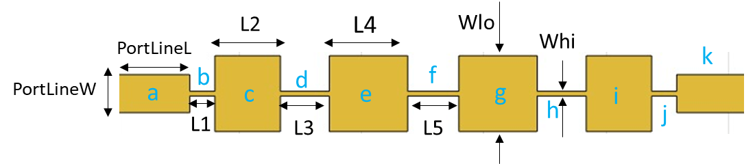
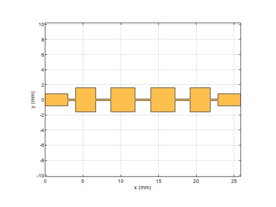
Whi = 0.2e-3;
Wlo = 3.2e-3;
L1  = 1.02e-3;
L2  = 2.67e-3;
L3  = 2e-3;
L4  = 3.2e-3;
L5  = 2.09e-3;

a = traceRectangular('Length',PortLineL,'Width',PortLineW,'Center',[PortLineL/2,0]);
b = traceRectangular('Length',L1,'Width',Whi,'Center',[PortLineL+L1/2,0]);
c = traceRectangular('Length',L2,'Width',Wlo,'Center',[PortLineL+L1+L2/2,0]);
d = traceRectangular('Length',L3,'Width',Whi,'Center',[PortLineL+L1+L2+L3/2,0]);
e = traceRectangular('Length',L4,'Width',Wlo,'Center',[PortLineL+L1+L2+L3+L4/2,0]);
f = traceRectangular('Length',L5,'Width',Whi,'Center',[PortLineL+L1+L2+L3+L4+L5/2,0]);
g = traceRectangular('Length',L4,'Width',Wlo,'Center',[PortLineL+L1+L2+L3+L4+L5+L4/2,0]);
h = traceRectangular('Length',L3,'Width',Whi,'Center',[PortLineL+L1+L2+L3+L4+L5+L4+L3/2,0]);
i = traceRectangular('Length',L2,'Width',Wlo,'Center',[PortLineL+L1+L2+L3+L4+L5+L4+L3+L2/2,0]);
j = traceRectangular('Length',L1,'Width',Whi,'Center',[PortLineL+L1+L2+L3+L4+L5+L4+L3+L2+L1/2,0]);
k = traceRectangular('Length',PortLineL,'Width',PortLineW,'Center',[PortLineL+L1+L2+L3+L4+L5+L4+L3+L2+L1+PortLineL/2,0]);
filt1 = a+b+c+d+e+f+g+h+i+j+k;
figure,show(filt1);
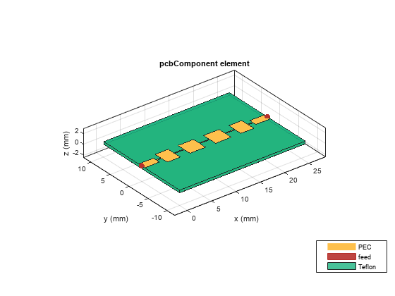
Create the PCB Stack of the filter using the pcbComponent object. Assign the filter shape, dielectric, and groundplane to the Layers property. Set the BoardThickness to 0.508 mm and assign the BoardShape to the ground plane. Set the FeedDiameter and FeedLocations. Visualize the PCB.
LPF                = pcbComponent;
d                  = dielectric('Teflon');
d.EpsilonR         = 2.2;
d.Thickness        = 0.508e-3;
d.FrequencyModel   = "DjordjevicSarkar";
GPL1               = PortLineL+L1+L2+L3+L4+L5+L4+L3+L2+L1+PortLineL;
GPW                = 20e-3;
gnd                = traceRectangular('Length',GPL1,'Width',GPW,'Center',[GPL1/2,0]);
LPF.BoardThickness = 0.508e-3;
LPF.Layers         = {filt1,d,gnd};
LPF.BoardShape     = gnd;
LPF.FeedDiameter   = PortLineW/2;
LPF.FeedLocations  = [0,0,1,3;GPL1,0,1,3];
figure,show(LPF);
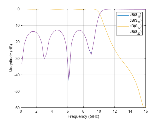
Use sparameters function to calculate the S-Parameters of the filter. Choose the adaptive interpolating sweep to compute the s-parameters over a finely discretized frequency range consisting of 200 points between 100 MHz and 16 GHz. Plot the s-parameters using the rfplot function.
spar1 = sparameters(LPF,linspace(0.1e9,16e9,200),'SweepOption','interp');
figure;
rfplot(spar1);
The adaptive sweep allows for characterizing the s-parameter performance by calculating the full-wave solution only at a fraction of the frequency points provided as the input. To understand the advantage of this approach, use the info function to see the frequencies at which a full-wave solution was calculated.
ILPfilt = info(LPF)
ILPfilt = struct with fields:
          IsSolved: "true"
          IsMeshed: "true"
       MeshingMode: "auto"
      HasSubstrate: "true"
           HasLoad: "false"
     PortFrequency: [1.6000e+10 100000000 8.0500e+09 1.0795e+08 1.1591e+08 1.1196e+10 1.5992e+10 1.3647e+09 1.2397e+10 2.4385e+09 1.0146e+10 5.8428e+09 8.3244e+09 6.7177e+09 6.9007e+09 9.4777e+09 1.3876e+10 1.3773e+10 1.3781e+10 … ] (1×27 double)
    MemoryEstimate: "820 MB"
Nfullwave = numel(ILPfilt.PortFrequency)
Nfullwave =
27
For this low pass filter structure, only 35 frequencies were used to fully characterize the performance. Note, also that the frequencies are chosen in an adaptive way so as to produce a highly accurate rational model.
High Pass Filter
Create the variables and assign the values given in the paper[1]. Use the traceRectangular shape to create all the rectangles as shown in the figure and join them to create the filter structure. Visualize the structure using the show function.

Lstub = 6.35e-3;
Wstub = 0.238e-3;
Linv  = 6.07e-3;
Winv  = 1.8e-3;
a = traceRectangular('Length',PortLineL,'Width',PortLineW,'Center',[PortLineL/2,0]);
b = traceRectangular('Length',Linv,'Width',Winv,'Center',[PortLineL+Linv/2,0]);
c = traceRectangular('Length',Linv+0.04e-3,'Width',Winv,'Center',[PortLineL+Linv+Linv/2+0.04e-3/2,0]);
d = traceRectangular('Length',PortLineL+0.1e-3,'Width',PortLineW,'Center',[PortLineL+Linv+Linv+PortLineL/2-0.1e-3/2,0]);
e = traceRectangular('Length',Wstub,'Width',Lstub,'Center',[PortLineL+Wstub/2,-Lstub/2-PortLineW/2]);
f = traceRectangular('Length',Wstub,'Width',Lstub,'Center',[PortLineL+Linv+Wstub/2,-Lstub/2-PortLineW/2]);
g = traceRectangular('Length',Wstub,'Width',Lstub,'Center',[PortLineL+Linv+Linv+Wstub/2,-Lstub/2-PortLineW/2]);
filt2 = a+b+c+d+e+f+g;
figure;
show(filt2);
Create the PCB Stack of the filter using the pcbComponent. Assign the filter shape, dielectric, and groundplane to the Layers property. Set the BoardThickness to 0.508 mm and assign the BoardShape to the ground plane. Set the FeedDiameter and FeedLocations. Visualize the PCB.
HPF                = pcbComponent;
d                  = dielectric('Teflon');
d.EpsilonR         = 2.2;
d.Thickness        = 0.508e-3;
d.FrequencyModel   = "DjordjevicSarkar";
GPL2               = PortLineL+Linv+Linv+PortLineL;
GPW                = 20e-3;
gnd                = traceRectangular('Length',GPL2,'Width',GPW,'Center',[GPL2/2,0]);
HPF.BoardThickness = 0.508e-3;
HPF.Layers         = {filt2,d,gnd};
HPF.BoardShape     = gnd;
HPF.FeedDiameter   = PortLineW/2;
HPF.FeedLocations  = [0,0,1,3;GPL2,0,1,3];
HPF.ViaLocations   = [PortLineL+Wstub/2,-PortLineW/2-Lstub+0.2e-3,1,3;PortLineL+Linv+Wstub/2,-PortLineW/2-Lstub+0.2e-3,1,3;PortLineL+Linv+Linv+Wstub/2,-PortLineW/2-Lstub+0.2e-3,1,3];
HPF.ViaDiameter    = Wstub/2;
figure;
show(HPF);
Use sparameters function to calculate the s-parameters of the filter, with a frequencySweep object to set up the frequency sweep. Use a gradient-based adaptive interpolating sweep and set the error tolerance to -100 dB with a maximum number of 40 iterations for the fit to be calculated. As before, plot the s-parameters using the rfplot function.
fsHPF = frequencySweep;
fsHPF.SweepType = 'interpWithGrad';
fsHPF.ErrTol = -100;
fsHPF.NumIters = 40;
spar2 = sparameters(HPF,linspace(0.1e9,20e9,200),'SweepOption',fsHPF);
figure;
rfplot(spar2);
Cascaded Filter Response
Cascade the LPF and HPF created above and create a ground plane so that it supports the cascaded shape.
filt12   = translate(copy(filt1),[-GPL1,0,0]);
filtcasc = filt12+filt2;
figure,show(filtcasc);
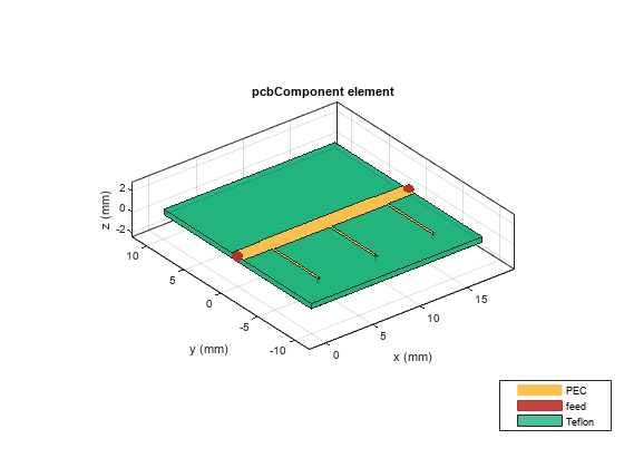
Create the PCB Stack of the filter using the pcbComponent. Create the groundplane using the traceRectangular shape. Assign the filter shape, dielectric, and groundplane to the Layers property. Set the BoardThickness to 0.508 mm and assign the BoardShape to the ground plane. Set the FeedDiameter and FeedLocations. Visualize the PCB.
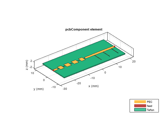
casc                = pcbComponent;
d                   = dielectric('Teflon');
d.EpsilonR          = 2.2;
d.Thickness         = 0.508e-3;
d.FrequencyModel    = "DjordjevicSarkar";
GPL  = GPL1+GPL2;
GPW  = 20e-3;
gnd  = traceRectangular('Length',GPL,'Width',GPW,'Center',[(-GPL1+GPL2)/2,0]);
GPL3                = PortLineL+Linv+Linv+PortLineL;
casc.BoardThickness = 0.508e-3;
casc.Layers         = {filtcasc,d,gnd};
casc.BoardShape     = gnd;
casc.FeedDiameter   = PortLineW/2;
casc.FeedLocations  = [-GPL1,0,1,3;GPL3,0,1,3];
casc.ViaLocations   = [PortLineL+Wstub/2,-PortLineW/2-Lstub+0.2e-3,1,3;PortLineL+Linv+Wstub/2,-PortLineW/2-Lstub+0.2e-3,1,3;PortLineL+Linv+Linv+Wstub/2,-PortLineW/2-Lstub+0.2e-3,1,3];
casc.ViaDiameter    = Wstub/2;
figure;
show(casc);
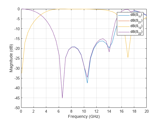
Use the sparameters function to calculate the S-Parameters and plot the parameters using the rfplot function
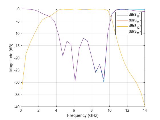
spar3 = sparameters(casc,linspace(0.1e9,14e9,200),'SweepOption','interp');
figure;
rfplot(spar3);
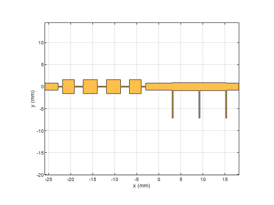
Composite Filter Type 1
Create the variables and assign the values given in the paper[1]. Use the traceRectangular shape to create all the rectangles as shown in the figure and join them to create the filter structure. Visualize the structure using the show function.
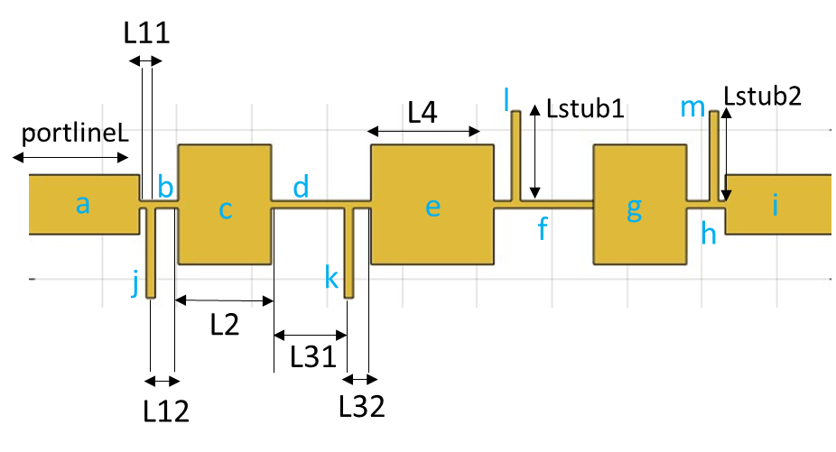
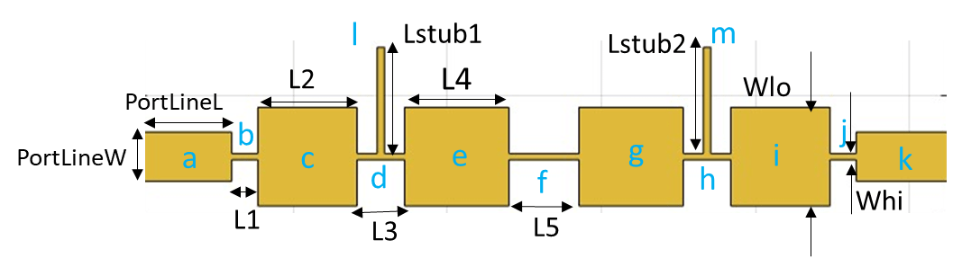
L11 = 0.3e-3;
L12 = 0.73e-3;
L2  = 2.48e-3;
L31 = 2.07e-3;
L32 = 0.59e-3;
L4  = 3.28e-3;
Lstub1 = 2.4e-3;
Lstub2 = 2.4e-3;
a = traceRectangular('Length',PortLineL,'Width',PortLineW,'Center',[PortLineL/2,0]);
b = traceRectangular('Length',L11+L12,'Width',Whi,'Center',[PortLineL+(L11+L12)/2,0]);
c = traceRectangular('Length',L2,'Width',Wlo,'Center',[PortLineL+L11+L12+L2/2,0]);
d = traceRectangular('Length',L31+L32,'Width',Whi,'Center',[PortLineL+L11+L12+L2+(L31+L32)/2,0]);
e = traceRectangular('Length',L4,'Width',Wlo,'Center',[PortLineL+L11+L12+L2+(L31+L32)+L4/2,0]);
f = traceRectangular('Length',L31+L32,'Width',Whi,'Center',[PortLineL+L11+L12+L2+(L31+L32)+L4+(L31+L32)/2,0]);
g = traceRectangular('Length',L2,'Width',Wlo,'Center',[PortLineL+L11+L12+L2+(L31+L32)+L4+(L31+L32)+L2/2,0]);
h = traceRectangular('Length',L11+L12,'Width',Whi,'Center',[PortLineL+L11+L12+L2+(L31+L32)+L4+(L31+L32)+L2+(L11+L12)/2,0]);
i = traceRectangular('Length',PortLineL,'Width',PortLineW,'Center',[PortLineL+L11+L12+L2+(L31+L32)+L4+(L31+L32)+L2+(L11+L12)+PortLineL/2,0]);
j = traceRectangular('Length',Wstub,'Width',Lstub1,'Center',[PortLineL+L11,-Lstub1/2-Whi/2]);
k = traceRectangular('Length',Wstub,'Width',Lstub1,'Center',[PortLineL+L11+L12+L2+L31,-Lstub1/2-Whi/2]);
l = traceRectangular('Length',Wstub,'Width',Lstub1,'Center',[PortLineL+L11+L12+L2+L31+L32+L4+L32,Lstub1/2+Whi/2]);
m = traceRectangular('Length',Wstub,'Width',Lstub1,'Center',[PortLineL+L11+L12+L2+L31+L32+L4+L32+L31+L2+L12,Lstub1/2+Whi/2]);
compfiltShape1 = a+b+c+d+e+f+g+h+i+j+k+l+m;
figure;
show(compfiltShape1);
Create the PCB Stack of the filter using the pcbComponent. Assign the filter shape, dielectric, and groundplane to the Layers property. Set the BoardThickness to 0.508 mm and assign the BoardShape to the ground plane. Set the FeedDiameter and FeedLocations. Visualize the PCB.
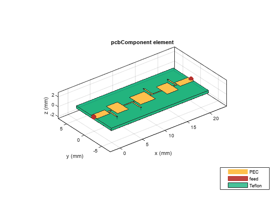
compfilt1 = pcbComponent;
d    = dielectric('Teflon');
d.EpsilonR  = 2.2;
d.Thickness = 0.508e-3;
d.FrequencyModel = "DjordjevicSarkar";
GPL2 = PortLineL+2*(L11+L12)+2*(L31+L32)+2*L2+L4+PortLineL;
GPW  = 20e-3;
gnd  = traceRectangular('Length',GPL2,'Width',GPW/2,'Center',[(GPL2)/2,0]);
compfilt1.BoardThickness = 0.508e-3;
compfilt1.Layers         = {compfiltShape1,d,gnd};
compfilt1.BoardShape     = gnd;
compfilt1.FeedDiameter   = PortLineW/2;
compfilt1.FeedLocations  = [0,0,1,3;GPL2,0,1,3];
compfilt1.ViaLocations   = [PortLineL+L11,-Whi/2-Lstub1+0.1e-3,1,3;PortLineL+L11+L12+L2+L31,-Whi/2-Lstub1+0.1e-3,1,3;PortLineL+L11+L12+L2+L31+L32+L4+L32,Whi/2+Lstub1-0.1e-3,1,3;PortLineL+L11+L12+L2+L31+L32+L4+L32+L31+L2+L12,Whi/2+Lstub1-0.1e-3,1,3];
compfilt1.ViaDiameter    = Wstub/2;
figure;
show(compfilt1);
Use the mesh function to generate a manual mesh with a MaxEdgeLength as 1 mm.
figure;
mesh(compfilt1,'MaxEdgeLength',1e-3);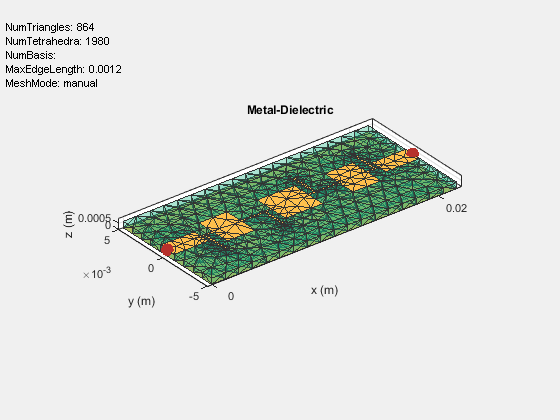
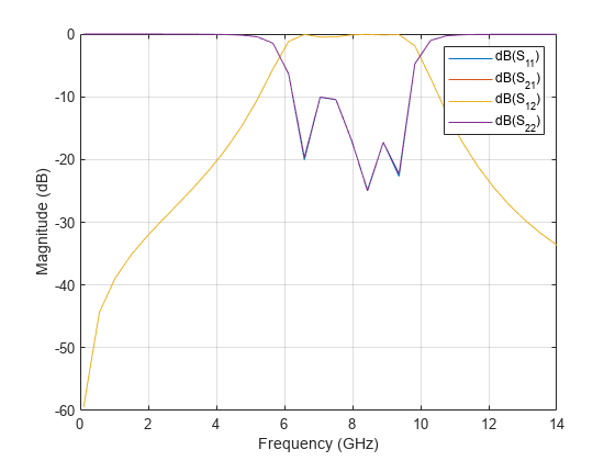
Use the sparameters function with the gradient-based adaptive interpolating sweep to calculate the s-parameters of the filter and plot them using the rfplot function.
spar4 = sparameters(compfilt1,linspace(0.1e9,14e9,300),'SweepOption','interpWithGrad');
figure;
rfplot(spar4);
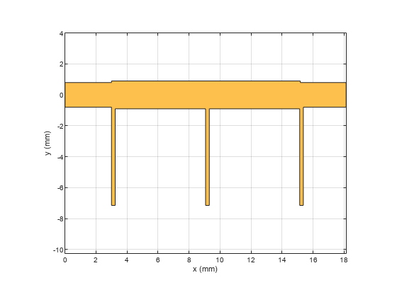
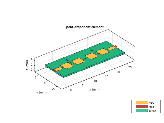
Composite Filter Type 2
Create the variables and assign the values given in the paper[1]. Use the traceRectangular shape to create all the rectangles as shown in the figure and join them to create the filter structure. Visualize the structure using the show function.
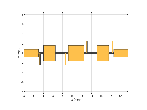
Whi = 0.2e-3;
Wlo = 3.2e-3;
L1  = 0.85e-3;
L2  = 3.22e-3;
L3  = 1.54e-3;
L4  = 3.39e-3;
L5  = 2.27e-3;
Lstub1 = 3.45e-3;
a  = traceRectangular('Length',PortLineL,'Width',PortLineW,'Center',[PortLineL/2,0]);
b  = traceRectangular('Length',L1,'Width',Whi,'Center',[PortLineL+L1/2,0]);
c  = traceRectangular('Length',L2,'Width',Wlo,'Center',[PortLineL+L1+L2/2,0]);
l = traceRectangular('Length',Wstub,'Width',Lstub1,'Center',[PortLineL+L1+L2+L3/2,Lstub1/2+Whi/2]);
d  = traceRectangular('Length',L3,'Width',Whi,'Center',[PortLineL+L1+L2+L3/2,0]);
e  = traceRectangular('Length',L4,'Width',Wlo,'Center',[PortLineL+L1+L2+L3+L4/2,0]);
f  = traceRectangular('Length',L5,'Width',Whi,'Center',[PortLineL+L1+L2+L3+L4+L5/2,0]);
g  = traceRectangular('Length',L4,'Width',Wlo,'Center',[PortLineL+L1+L2+L3+L4+L5+L4/2,0]);
m = traceRectangular('Length',Wstub,'Width',Lstub1,'Center',[PortLineL+L1+L2+L3+L4+L5+L4+L3/2,Lstub1/2+Whi/2]);
h  = traceRectangular('Length',L3,'Width',Whi,'Center',[PortLineL+L1+L2+L3+L4+L5+L4+L3/2,0]);
i  = traceRectangular('Length',L2,'Width',Wlo,'Center',[PortLineL+L1+L2+L3+L4+L5+L4+L3+L2/2,0]);
j  = traceRectangular('Length',L1,'Width',Whi,'Center',[PortLineL+L1+L2+L3+L4+L5+L4+L3+L2+L1/2,0]);
k  = traceRectangular('Length',PortLineL,'Width',PortLineW,'Center',[PortLineL+L1+L2+L3+L4+L5+L4+L3+L2+L1+PortLineL/2,0]);
compfiltShape2 = a+b+c+d+e+f+g+h+i+j+k+l+m;
figure;
show(compfiltShape2);

Create the PCB Stack of the filter using the pcbComponent. Assign the filter shape, dielectric, and groundplane to the Layers property. Set the BoardThickness to 0.508 mm and assign the BoardShape to the ground plane. Set the FeedDiameter and FeedLocations. Visualize the PCB.
compfilt2 = pcbComponent;
d = dielectric('Teflon');
d.EpsilonR  = 2.2;
d.Thickness = 0.508e-3;
d.FrequencyModel = "DjordjevicSarkar";
GPL1 = PortLineL+L1+L2+L3+L4+L5+L4+L3+L2+L1+PortLineL;
GPW  = 20e-3;
gnd  = traceRectangular('Length',GPL1,'Width',GPW/2,'Center',[GPL1/2,0]);
compfilt2.BoardThickness = 0.508e-3;
compfilt2.Layers         = {compfiltShape2,d,gnd};
compfilt2.BoardShape     = gnd;
compfilt2.FeedDiameter   = PortLineW/2;
compfilt2.FeedLocations  = [0,0,1,3;GPL1,0,1,3];
compfilt2.ViaLocations   = [PortLineL+L1+L2+L3/2,Lstub1+Whi/2-0.2e-3,1,3;PortLineL+L1+L2+L3+L4+L5+L4+L3/2,Lstub1+Whi/2-0.2e-3,1,3];
compfilt2.ViaDiameter    = Wstub/2;
figure;
show(compfilt2);
Use the mesh function to generate a manual mesh with a MaxEdgeLength as 1.0 mm.
figure;
mesh(compfilt2,'MaxEdgeLength',1e-3);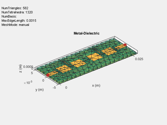
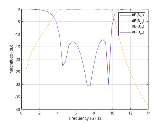
Use sparameters function to calculate the S-Parameters of the filter and plot them using the rfplot function.
spar5 = sparameters(compfilt2,linspace(0.5e9,14e9,300),'SweepOption','interpWithGrad');
figure;
rfplot(spar5);
References
1) Ching-Luh Hsu, Fu-Chieh Hsu and Jen-Tsai Kuo, Microstrip Bandpass Filters for Ultra-Wideband (UWB) Wireless Communications.