bendMitered
Description
Use the bendMitered object to create a mitered bend shape on the
X-Y plane.
Note
This shape object supports behavioral modeling. For more information, see Behavioral Models.
Creation
Description
bend = bendMitered creates a mitered bend shape on the X-Y
plane.
bend = bendMitered(
sets Properties using one or more
name-value arguments. For example, PropertyName=Value)bendMitered(ReferencePoint=[1 1])
creates a mitered bend shape with the reference point at [1 1].
Properties not specified retain their default values.
Properties
Object Functions
add | Boolean unite operation on two RF PCB shapes |
and | Shape1 & Shape2 for RF PCB shapes |
area | Calculate area of RF PCB shape in square meters |
intersect | Boolean intersection operation on two RF PCB shapes |
mesh | Change and view mesh properties of metal or dielectric in PCB component |
minus | Shape1 - Shape2 for RF PCB shapes |
mirrorX | Mirror shape along X-axis |
mirrorY | Mirror shape along Y-axis |
plus | Shape1 + Shape2 for RF PCB shapes |
rotate | Rotate RF PCB shape about defined axis |
rotateX | Rotate RF PCB shape about x-axis |
rotateY | Rotate RF PCB shape about y-axis and angle |
rotateZ | Rotate RF PCB shape about z-axis |
subtract | Boolean subtraction operation on two RF PCB shapes |
scale | Change size of RF PCB shape by fixed amount |
show | Display PCB component structure or PCB shape |
translate | Move RF PCB shape to new location |
Examples
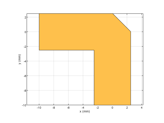
Create a mitered bend with default properties.
bend = bendMitered
bend =
  bendMitered with properties:

              Name: 'myMiteredbend'
    ReferencePoint: [0 0]
            Length: [0.0100 0.0100]
             Width: [0.0050 0.0050]
     MiterDiagonal: 0.0035
View the shape.
show(bend)
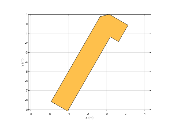
Create a mitered bend shape of lengths of 10 m and 2 m, width of 2 m, and rotate it about the Z-axis by 60 degrees.
bend = bendMitered(Length=[10 2],Width=[2 2],MiterDiagonal=1);
bend = rotateZ(bend,60)
bend =
  bendMitered with properties:

              Name: 'myMiteredbend'
    ReferencePoint: [0 0]
            Length: [10 2]
             Width: [2 2]
     MiterDiagonal: 1
show(bend)
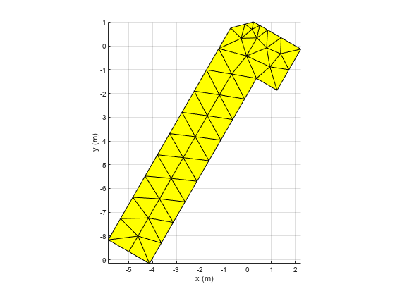
Mesh the mitered bend shape at a maximum edge length of 1 m.
mesh(bend,MaxEdgeLength=1)
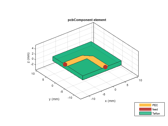
Create mitered bend microstrip.
m = design(microstripLine,6e9,"Z0",75);
layer2d = bendMitered('Length',[m.Length/2 m.Length/2],...
"Width",[m.Width m.Width],'MiterDiagonal',sqrt(2)*m.Width);
robj = pcbComponent(layer2d);
robj.BoardThickness = m.Substrate.Thickness;
robj.Layers{2} = m.Substrate;
show(robj)
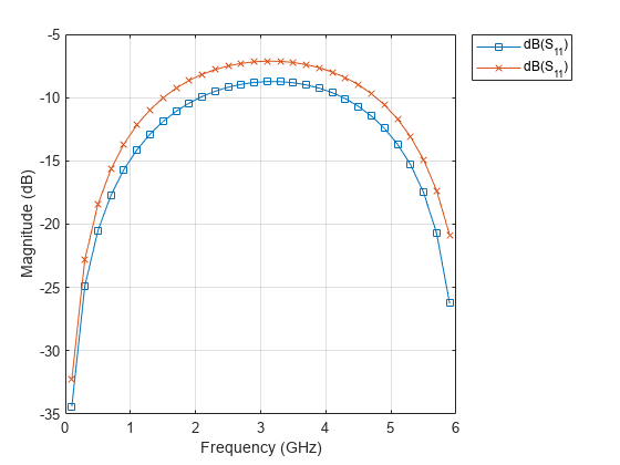
Compute and plot s-parameters.
freq = (1:2:60)*100e6;
Sckt = sparameters(robj,freq,'Behavioral',true);
Sem = sparameters(robj,freq);
rfplot(Sckt,1,1,'db','-s')
hold on
rfplot(Sem,1,1,'db','-x')
Reference:
M. Kirschning, R. H. Jansen and N. H. L. Koster, "Measurement and Computer-Aided Modeling of Microstrip Discontinuities by an Improved Resonator Method," 1983 IEEE MTT-S International Microwave Symposium Digest, Boston, MA, USA, 1983, pp. 495-497, doi: 10.1109/MWSYM.1983.1130959.
Version History
Introduced in R2021b