Design, Analyze, and Export 1-by-2 H-Notch Linear Array
This step of the tutorial shows how to design, analyze, and export a 1-by-2 H-notch linear array.
Design 1-by-2 H-Notch Linear Antenna Array
Select HNotchLayer in the PCB Stack pane and drag the axes to create a selection box. Drag the axes until the selection box encloses Feed and HNotchLayer.

Click Copy on the Design tab to copy the layers enclosed in the selection box and click Paste to create the HPatch_Copy(1) layer.

Select the HPatch_Copy(1) layer and drag it to place it to adjacent to the HPatch layer.
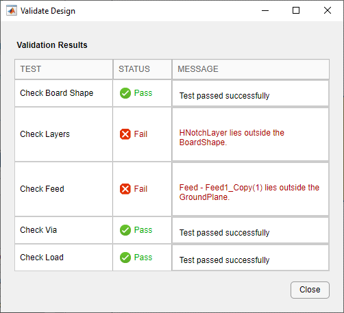
Validate Design for Errors
Click Validate Design on the toolbar to validate your board shape, layers, feed, via, and load. The Check Layers and Check Feed validation failed because HNotchLayer and Feed1_Copy(1) lie outside BoardShape and GroundPlane, respectively.
Overlay Layers
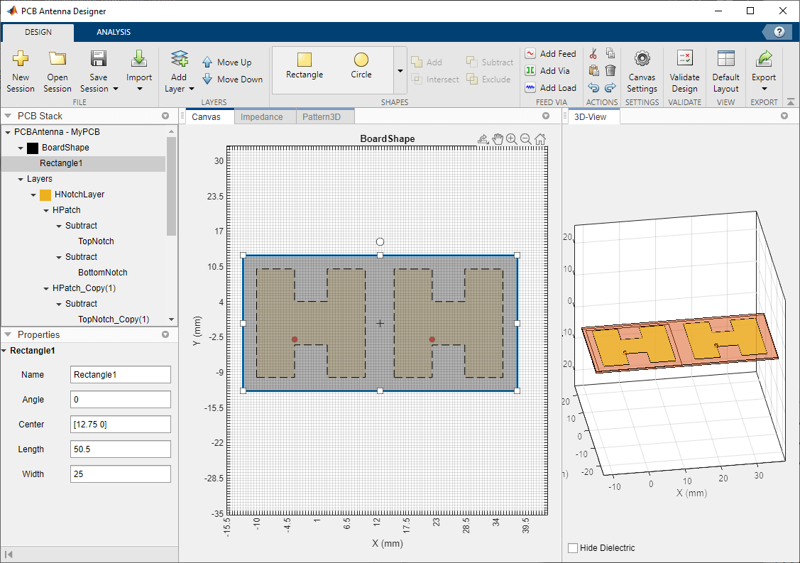
Select HNotchLayer and then select the Overlay check box in the Properties pane to create an image of HNotchLayer in the canvas.

Select Rectangle1 under BoardShape on the canvas and use the marker on the right to change the shape of BoardShape such that it encloses the HNotch image.
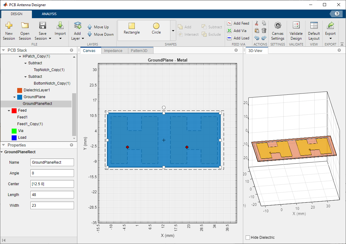
Repeat the procedure with the GroundPlane layer.
The BoardShape now encloses the HNotchLayer. You can change the layer dimensions using the Properties pane.
Validate Design for Errors
Click Validate Design to check for issues in the design. The design is validated with no errors.

Run Analysis
Click Update Plots in the Analysis tab to update the analysis results. This updates all the analysis plots in the app for the design of a 1-by-2 H-notch linear array.
3-D Pattern
The pattern for the antenna is more directional with a higher gain compared to the H-notch patch unit element. The directivity of the 1-by-2 H-notch linear array is 7.66 dBi.

Export Your Design to Gerber Files
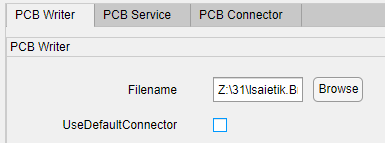
In the Analysis tab, click Export and then select Export as Gerber File. In the Gerber Export dialog box, select Browse in the PCB Writer tab to select the directory in which you want the Gerber files to be stored.

Clear the UseDefaultConnector check box.

In the PCB Services tab, under Services, select GerbLookWriter. The PCB writer uses the selected service to create the Gerber files.
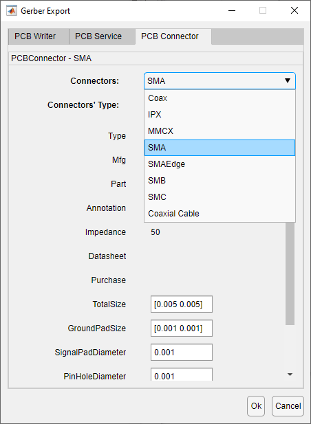
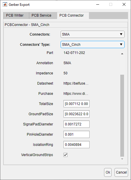
In the PCB Connector tab, set Connectors to SMA and Connectors' Type to SMA_Cinch.

The PinHoleDiameter is of the same value as the FeedDiameter. Click OK to generate the Gerber files.
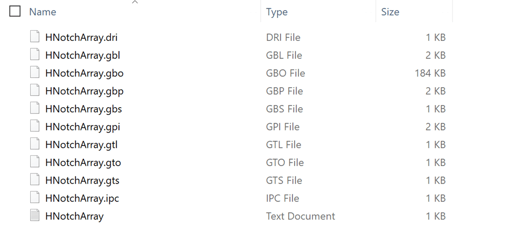
The generated Gerber files are stored as a .zip file in the directory that you selected in the PCB Writer tab.
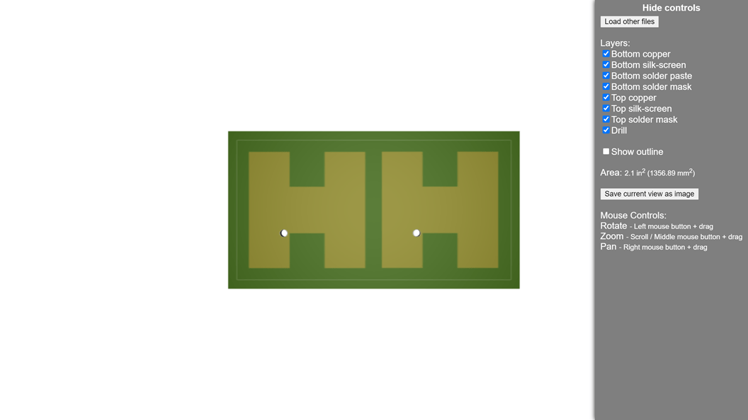
Open gerblook web Gerber interface from your browser. Click to upload, or drag and drop the zip-file from the directory.

The Gerber files are displayed in the Gerber viewer. You can use the Gerber files to fabricate your 1-by-2 H-notch linear array.
All the layers overlayed:

Top Layer:
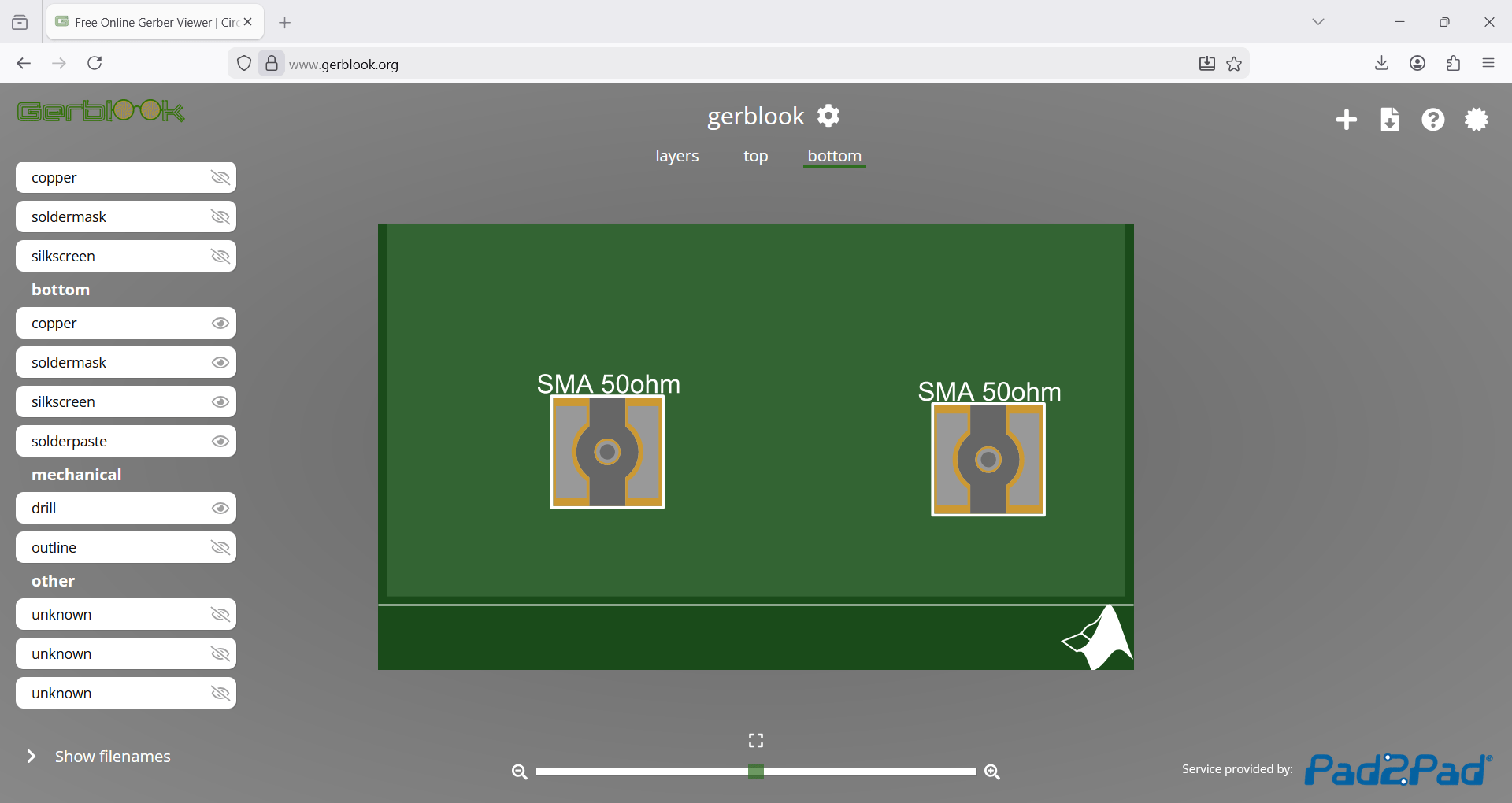
Bottom Layer:
You can also export your design to the MATLAB® workspace or MATLAB script by selecting Export to MATLAB Workspace or Export to MATLAB Script under Export in the Design or Analysis tab.