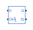
Main Content

D Flip-Flop

Behavioral model of D flip-flop

Since R2024a

  • D Flip-Flop block

Libraries:
Simscape / Electrical / Integrated Circuits / Logic

Description

The D Flip-Flop block implements a behavioral model of a clocked D flip-flop. The block stores a one-bit value, either 0 (low) or 1 (high).

The block has two input ports: the data pin D and the clock pin Clk. The block transfers the data at D to the output pin Q. The output updates only when the clock signal transitions on the active edge of the clock. Otherwise, the block holds the output in its previous state.

You can update the output on the falling or rising edge of the clock. To update the output only when the clock transitions from high to low, set the Edge trigger parameter to Falling. To update the output only when the clock transitions from low to high, set the Edge trigger parameter to Rising. This truth table summarizes the logic levels at the inputs and output. The subscript n represents the value at the current clock cycle and n-1 represents the value at the previous clock cycle. The logic level at the inverted output pin !Q is the inverse of the logic level at Q.

Edge trigger parameter valueClkn-1ClknQn
Falling00Qn-1
Falling01Qn-1
Falling10Dn
Falling11Qn-1
Rising00Qn-1
Rising01Dn
Rising10Qn-1
Rising11Qn-1

To specify the logic level at Q at the start of the simulation, in the Initial Targets section, set the value of the Output logic parameter to 0 or 1. For more information about initial targets, see Set Priority and Initial Target for Block Variables.

The gate inputs have an infinite resistance and a finite or zero capacitance.

If the gate voltage is greater than the threshold voltage, then the block takes the logic level at the input as 1. Otherwise, the block takes the logic level at the input as 0. The block calculates the threshold voltage as the average of the Low level input voltage and the High level input voltage parameter values.

The gate output depends on the Output current-voltage relationship parameter. Set this parameter to Linear for faster simulation and Quadratic for more accurate results. For most models, use the Linear option. You can use the Quadratic option to validate the results that you obtain using the simpler linear model. For more information, see Selecting the Output Model for Logic Blocks.

If you set the Output current-voltage relationship parameter to Linear:

  • If the logic level at the Q port is 0, the output voltage is equal to the Low level output voltage parameter value.

  • If the logic level at the Q port is 1, the output voltage is equal to the High level output voltage parameter value.

  • The resistor-capacitor time constant of the gate output capacitor is equal to the Propagation delay parameter value.

If you set the Output current-voltage relationship parameter to Quadratic:

  • The output voltage is a function of the output current. For zero-load current:

    • If the logic level at the Q port is 0, the output voltage is zero.

    • If the logic level at the Q port is 1, the output voltage is equal to the Supply voltage parameter value.

  • The gate input demand lags to approximate the Propagation delay parameter value.

For more information, see Quadratic Model Output and Parameters.

Plot Input and Output Waveforms

You can plot the input and output waveforms of the D Flip-Flop block without building a complete model. Use the plots to explore the impact of your parameter choices on device characteristics. If you parameterize the block from a datasheet, you can compare your plots to the datasheet to check that you parameterized the block correctly. If you have a complete working model but do not know which manufactured part to use, you can compare your plots to datasheets to help you decide.

To plot the basic characteristics, right-click the block and select Electrical > Basic characteristics from the context menu.

Note

The plots you create using the Basic characteristics option do not show the effect of the Propagation delay parameter on the output voltage of logic blocks.

Assumptions and Limitations

  • To improve simulation speed, the block does not model all the internal metal-oxide-semiconductor field-effect transistor (MOSFET) devices in the gate individually. The block therefore does not accurately model the response of the gate to input noise and input voltages that are close to the threshold voltage.

  • If you are modeling a circuit that has a feedback path around a set of logic gates, you must set the Propagation delay parameter to a nonzero value on one or more of the gates.

Ports

Output

expand all

Output validity port. The value of the physical signal is 1 during setup and hold time. Under these conditions, the output of the real D flip-flop hardware is unpredictable. Otherwise, the value of this physical signal is 0.

Dependencies

To enable this port, select the Expose output validity port parameter.

Conserving

expand all

Electrical conserving port associated with the data pin.

Electrical conserving port associated with the clock pin.

Electrical conserving port associated with the output pin.

Electrical conserving port associated with the inverted output pin.

Parameters

expand all

To edit block parameters interactively, use the Property Inspector. From the Simulink® Toolstrip, on the Simulation tab, in the Prepare gallery, select Property Inspector.

Inputs

Input voltage below which the block interprets the input logic as 0.

Input voltage above which the block interprets the input logic as 1.

Fixed capacitance that approximates the input capacitance for a MOSFET gate. The MOSFET capacitance depends on the applied voltage. When you drive this block with another gate, the Average input capacitance parameter produces a rise time similar to that of the MOSFET. You can find this capacitance value on a manufacturer datasheet. For fast simulation, set this parameter to zero.

Trigger for the active edge of the clock. To update the output only when the logic level at the Clk port transitions from 1 to 0, set the Edge trigger parameter to Falling. To update the output only when the logic level at the Clk port transitions from 0 to 1, set the Edge trigger parameter to Rising.

Outputs

Model that determines the relationship between the output current and output voltage. Set this parameter to Linear for faster simulation and Quadratic for more accurate results. For more information, see Selecting the Output Model for Logic Blocks.

Output voltage when the logic level at the output pin is 0.

Dependencies

To enable this parameter, set Output current-voltage relationship to Linear.

Output voltage when the logic level at the output pin is 1.

Dependencies

To enable this parameter, set Output current-voltage relationship to Linear.

Output resistance that the block uses to model the drop in output voltage resulting from the output current. You can calculate this value from a datasheet by dividing the high-level output voltage by the maximum low-level output current.

If you set the Propagation delay parameter to zero, you must set the Output resistance parameter to a positive value.

Dependencies

To enable this parameter, set Output current-voltage relationship to Linear.

Voltage you supply to the gate in the circuit.

Dependencies

To enable this parameter, set Output current-voltage relationship to Quadratic.

Gate supply voltage at which you quote the output resistances and currents.

Dependencies

To enable this parameter, set Output current-voltage relationship to Quadratic.

Resistance when the logic level at the output is 1. Specify this parameter as a row vector of two resistance values [R_OH1, R_OH2]. The first value, R_OH1, is the gradient of the output voltage-current relationship when there is no output current. The second value, R_OH2, is the gradient of the output voltage-current relationship when the output is shorted to ground.

Dependencies

To enable this parameter, set Output current-voltage relationship to Quadratic.

Output current when the logic level at the output is 1, but the load forces the output voltage to zero.

Dependencies

To enable this parameter, set Output current-voltage relationship to Quadratic.

Resistance when the logic level at the output is 0. Specify this parameter as a row vector of two resistance values [R_OL1, R_OL2]. The first value, R_OL1, is the gradient of the output voltage-current relationship when there is no output current. The second value, R_OL2, is the gradient of the output voltage-current relationship when the load forces the output voltage to the Supply voltage parameter value.

Dependencies

To enable this parameter, set Output current-voltage relationship to Quadratic.

Output current when the logic level at the output is 0, but the load forces the output voltage to the Supply voltage parameter value.

Dependencies

To enable this parameter, set Output current-voltage relationship to Quadratic.

Time it takes for the output voltage to change from the low to high or high to low states after the input logic levels change.

If you set the Propagation delay parameter to zero, you must set the Output resistance parameter to a positive value.

Minimum amount of time before a transition, on the active edge of the clock, that the input data must be stable for the latches of the flip-flop to latch correctly.

Minimum amount of time after a transition, on the active edge of the clock, that the input data must be stable for the latches of the flip-flop to latch correctly.

Gradient of the voltage-current relationship for the protection diodes when they are forward biased.

Dependencies

To enable this parameter, set Output current-voltage relationship to Quadratic.

Voltage above which the protection diode turns on.

Dependencies

To enable this parameter, set Output current-voltage relationship to Quadratic.

Option to expose the Invalid port.

Extended Capabilities

C/C++ Code Generation
Generate C and C++ code using Simulink® Coder™.

Version History

Introduced in R2024a