Guidelines for Clock and Reset Signals
In the Simulink® modeling environment, you do not create global signals such as clock, reset, and clock enable. These signals are created when you generate HDL code for your model. You can specify the clock cycle by using the sample time in Simulink.
If your model is single rate, it means all blocks operate at the same sample time. The synthesis tools infer that the registers or Delay blocks you add to your model run at the clock rate. For the synthesis tools, data propagates from the source register to the destination register in one clock cycle.
You can follow these guidelines to learn about generating clock signals in the HDL code. Each guideline has a severity level that indicates the level of compliance requirements. To learn more, see HDL Modeling Guidelines Severity Levels.
Use Global Oversampling to Create Frequency-Divided Clock
Guideline ID
1.4.1
Severity
Informative
Description
You can configure the Oversampling factor in HDL Code
Generation > Global Settings > Clock Settings that defines how
faster the global clock runs compared to the base sample rate of your model. The
default value is 1 (no oversampling). You can use oversampling when your DUT
functions within a larger system that uses a global clock to control timing, the
global clock often runs faster than some of its components. Instead of inserting
Upsample or Downsample blocks, you can integrate the DUT by specifying a global
oversampling clock. For example, if your model operates at a base sample time of
1 µs and you set Oversampling factor
= 10. Then the generated HDL clock runs at 100 ns, which is
10 times faster than the model rate.
You explicitly define an oversampling factor to set the global clock rate as a multiple of the model’s base rate. HDL Coder™ generates the global oversampling clock and derives the necessary timing signals from it. This global clock influences only the generated HDL code and does not affect the simulation behavior of your model. For more information, see Generate a Global Oversampling Clock.
Alternatively, you can also let HDL Coder automatically set an oversampling value based on your Simulink model rates and the Target Frequency parameter value during HDL code generation by enabling Treat Simulink rates as actual hardware rates parameter in model’s setting. Use this parameter, if you have complex feedback loops with multiple optimizations enabled for your model and you want the fastest data rate possible while allowing the optimizations to perform.
For example, if the Simulink base rate is 1 MHz and you want the clock
frequency of your target hardware to run at 50 MHz, you can set Target
Frequency to 50 and enable Treat
Simulink rates as actual hardware rates to allow HDL Coder
determine an optimized oversampling value that achieves your desired clock
frequency.
Create Multirate Model with Integer Clock Multiples by Clock Division
Guideline ID
1.4.2
Severity
Mandatory
Description
You can generate a multirate model by using clock-rate division or by using clock multiples. For a multirate model, the fastest sample time in your Simulink® model corresponds to the primary clock rate. A timing controller entity is created to control the clocking for blocks operating at slower sample rates. Clock enable signals that have the necessary rate and phase information control the clocking for these blocks in your design.
Multirate models are created when you use certain blocks in your Simulink model, specify certain block architectures, or use operations such as resource sharing. For example, these block-architecture combinations generate a multirate model:
Divide block with Newton-Raphson implementation.
Reciprocal block with ReciprocalSqrtBasedNewton implementation.
Sum of Elements and Product of Elements blocks with Cascade architecture.
Sqrt with SqrtBasedNewton and Reciprocal Sqrt with ReciprocalSqrtBasedNewton implementation.
In addition, to model multirate designs in Simulink, use these blocks:
In the Simulink > Signal Attributes Library, use the Rate Transition block.
In the DSP System Toolbox > Signal Operations Library, you can use Upsample, Downsample, and Repeat blocks.
In the HDL Coder > HDL RAMs Library, use the HDL FIFO block.
This model illustrates how to create a multirate design by using a Rate Transition block.
load_system('hdlcoder_multiclock')
set_param('hdlcoder_multiclock','SimulationCommand','Update')
open_system('hdlcoder_multiclock')
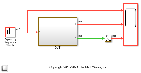
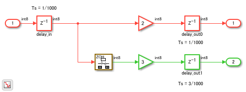
The different colors in the model indicate that the model is multirate and has a faster rate D1 and a slower rate D2. To see the Rate Transition block that produces the different sample rates, double-click the DUT Subsystem.
open_system('hdlcoder_multiclock/DUT')
To see the sample times in your model, run this command:
ts = Simulink.BlockDiagram.getSampleTimes('hdlcoder_multiclock');
sampletime_D1 = ts(1)
sampletime_D2 = ts(2)
sampletime_D1 =

  SampleTime with properties:

                   Value: [1.0000e-03 0]
             Description: 'Discrete 1'
           ColorRGBValue: [1 0.2706 0.2275]
              Annotation: 'D1'
              OwnerBlock: []
    ComponentSampleTimes: [0×0 Simulink.SampleTime]


sampletime_D2 =

  SampleTime with properties:

                   Value: [0.0030 0]
             Description: 'Discrete 2'
           ColorRGBValue: [0.2275 0.7843 0.1922]
              Annotation: 'D2'
              OwnerBlock: []
    ComponentSampleTimes: [0×0 Simulink.SampleTime]
When you use a Rate Transition block in your model for multirate design, select the block parameters Ensure data integrity during data transfer and Ensure deterministic data transfer (maximum delay). Make sure the output sample rate is an integer multiple of the input sample rate.
For a multirate design, you can generate a single clock signal or multiple clock signals to control the clocking to blocks that operate at various sample rates. To specify this setting, in the Configuration Parameters dialog box, on the HDL Code Generation > Global Settings pane, specify the Clock inputs setting.
By default, Clock inputs is specified as single. A single clock is generated to control the clocking for all registers or Delay blocks in your model. The timing controller enable signals control the clocking to various blocks in your design. This mode can increase the power dissipation as a single, fastest clock is connected to all registers in your design.
If you specify Clock inputs as multiple, a clock signal is generated for each sample rate in your design. However, this mode requires you to connect each of the clock, clock enable, and reset ports externally. This mode reduces power as the HDL design contains registers connected to slower clock signals. For more information, see Using Multiple Clocks in HDL Coder.
Use Dual Rate Dual Port RAM for Noninteger Multiple Sample Times
Guideline ID
1.4.3
Severity
Mandatory
Description
When you use Rate Transition, Upsample, or Downsample blocks to create multirate models, the clock rates must be integer multiples of the base rate. To create a multirate model with clocks that are noninteger multiples, use a Dual Rate Dual Port RAM block. For integer clock multiplies, you can use the HDL FIFO or the Dual Rate Dual Port RAM block.
This model illustrates how you can create noninteger multiples of sample rates.
load_system('hdlcoder_dual_rate_dual_port_RAM')
set_param('hdlcoder_dual_rate_dual_port_RAM','SimulationCommand','Update')
open_system('hdlcoder_dual_rate_dual_port_RAM/DUT')
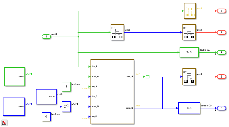
You cannot generate HDL code for this model because the Rate Transition blocks have the block parameter Ensure data integrity during data transfer cleared. To learn how you can manage address control when you use the RAM block, see Design Considerations for RAM Blocks and Blocks in HDL Operations Library.
Asynchronous Clock Modeling in HDL Coder
Guideline ID
1.4.4
Severity
Recommended
Description
Most FPGA designs must have more than one clock domain with multiple parts of the design operating at various frequencies. You can model the various clock domains in Simulink® by using a pass-through implementation for transitioning between different sample rates. These sample rates correspond to the clock rates on the FPGA device.
For an example, open the model hdlcoder_multi_clock_domain and then open the DUT Subsystem.
load_system('hdlcoder_multi_clock_domain')
set_param('hdlcoder_multi_clock_domain', 'SimulationCommand', 'Update')
open_system('hdlcoder_multi_clock_domain/DUT')
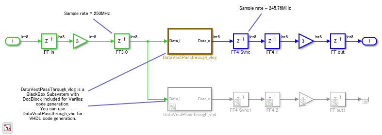
You see a BlackBox Subsystem that contains a DocBlock, which is a text file that corresponds to the Verilog® code for a passthrough implementation. You can open the DocBlock to see the Verilog code. You see that the output of this Subsystem operates at a different sample rate or is in a clock domain that is different from the sample rate at the input of the Subsystem. The Subsystem also contains a commented out path that contains the VHDL® equivalent of the passthrough implementation. To generate VHDL code, uncomment this path and comment out the path that contains the Verilog BlackBox implementation.
To generate Verilog code for this model, run this command:
makehdl('hdlcoder_multi_clock_domain/DUT')
In the generated Verilog header file, you see the different clock domains in the model.
// -------------------------------------------------------------
//
// File Name: hdlsrc\hdlcoder_multi_clock_domain\DUT.v
// Created: 2018-10-05 11:30:21
//
// Generated by MATLAB 9.6 and HDL Coder 3.13
//
//
// -- -------------------------------------------------------------
// -- Rate and Clocking Details
// -- -------------------------------------------------------------
// Model base rate: 1.30208e-12
// Target subsystem base rate: 2.65428e-12
//
//
// Clock      Domain  Description
// -- -------------------------------------------------------------
// clk_1_3072 1       3072x slower than base rate clock
// clk_1_3125 2       3125x slower than base rate clock
// -- -------------------------------------------------------------
//
// Output Signal                 Clock      Domain  Sample Time
// -- -------------------------------------------------------------
// Output1                       (no clock) 0       4.06901e-09
// -- -------------------------------------------------------------
//
// -------------------------------------------------------------
Use Global Reset Type Setting Based on Target Hardware
Guideline ID
1.4.5
Severity
Recommended
Description
Matching the reset type to the FPGA architecture can improve resource utilization and the speed at which your design runs on the target hardware. To control this setting, in the Configuration Parameters dialog box, on the HDL Code Generation > Global Settings settings, specify the Reset type.
When you target Xilinx® devices, set Reset type to
Synchronous. For Intel® or Altera® devices, set Reset type to
Asynchronous.
To make sure that you use the correct reset type for the hardware that you are targeting, in the HDL Code Advisor, run the model check Check for global reset setting for Xilinx and Altera devices.
Note
Some Intel devices recommend using synchronous reset. For recommended reset settings, see the Intel or Xilinx documentation for that device.
Define Sample Time in HDL Designs
Guideline ID
1.4.6
Severity
Recommended
Description
The sample time in Simulink models determines how the code generator generates the clock and enable signals. In HDL Coder, clock signals are not explicitly created in the Simulink model. When you generate HDL code, the code generator generates these signals based on the sample time and configuration settings of the model. In Simulink, each block has a sample time that determines how often it executes. HDL Coder uses this sample time to determine when the corresponding logic activates in hardware.
To set the sample time for a block, in the Block Parameters dialog box, use the Sample time parameter. Blocks that do not have Sample time parameter operate at base rate or at a rate respective to other sample rates in the model. HDL code generation supports only discrete sample times.
You can use the relative or absolute sample time for the model.
When you use relative sample times, a sample time of 1 is equivalent to one HDL clock cycle. Use relative sample times for abstract modeling or testing.
When you use absolute sample times, a sample time of 10e-9 is equivalent to 10 ns HDL clock cycles. Use absolute sample times for hardware-accurate modeling.
Follow these best practices:
For single-rate designs, use consistent sample times across blocks.
For multirate designs, use Rate Transition blocks to manage data transfer between blocks with different sample times.
To update your sample time and ratios more easily, use MATLAB variables (e.g.,
Ts = 10e-9,upsamp = 4) to define the sample times and ratios for easier updates.When designing hardware-accurate models, use realistic sample times (e.g.,
1e-6,1e-7) in your HDL designs.
Defining a sample time that matches your desired target frequency does not guarantee an actual clock speed on hardware. Actual clock frequency is limited by logic gate delays, routing delays, and critical path timing. HDL Coder can estimate these delays and provide feedback from RTL synthesis tools.
HDL Coder does not directly generate a clock signal based on sample time. It uses the sample time to determine:
The clock enable rate for each block
The timing controller logic for multirate designs
The oversampling factor when you specify target clock frequency
A multirate model contains multiple synchronous sample rates. You can use sample time colors and the sample time legend in the Simulink toolstrip under Debug > Information Overlays > Sample Time to visualize the different sample rates in the model. The fastest sample rate always appears in red.