Build and Simulate a Simple Circuit
This example shows how to build and simulate a simple circuit and view the results. You model a classic circuit configuration consisting of an integrator and a noninverting amplifier to generate the triangle wave. You use datasheets to specify block parameters and then look at the voltage at the wave generator output. To see the completed model, open the Model Triangle Wave Generator Using Operational Amplifiers example.
Select Blocks to Represent System Components
First, you select the blocks to represent the input signal, the triangle wave generator, and the output signal display.
You model the triangle wave generator with a set of physical blocks. The wave generator consists of:
Two operational amplifier blocks
Resistors and a capacitor that work with the operational amplifiers to create the integrator and noninverting amplifier
Simulink-PS Converter and PS-Simulink Converter blocks whose function is to bridge the physical part of the model, which uses physical signals, and the rest of the model, which uses Simulink® signals.
You have a manufacturer datasheet for the two operational amplifiers you want to model. Later in the example, you use the datasheet to parameterize the Simscape™ Electrical™ Band-Limited Op-Amp block.
The following table describes the role of the blocks that represent the system components.
Block | Description |
|---|---|
| Sine Wave | Generates a sinusoidal signal that controls the resistance of the Variable Resistor block |
| Scope | Displays the triangular output wave |
| Simulink-PS Converter | Converts the sinusoidal Simulink signal to a physical signal |
| Solver Configuration | Defines solver settings that apply to all physical modeling blocks |
| PS-Simulink Converter | Converts the output physical signal to a Simulink signal |
| Capacitor | Works with an operational amplifier and resistor block to create the integrator |
| Resistor | Works with the operational amplifier and capacitor blocks to create the integrator and noninverting amplifier |
| Variable Resistor | Supplies a time-varying resistance that adjusts the gain of the integrator, which in turn varies the frequency and amplitude of the generated triangular wave |
| DC Voltage Source | Generates a DC reference signal for the operational amplifier block of the noninverting amplifier |
| Voltage Sensor | Converts the electrical voltage at the output of the integrator into a physical signal proportional to the current |
| Electrical Reference | Provides the electrical ground |
| Band-Limited Op-Amp | Works with the capacitor and resistor to create an integrator and a noninverting amplifier |
| Diode | Limits the output of the Band-Limited Op-Amp block, to make the output waveform independent of supply voltage |
Build the Model
Create a Simulink model, add blocks to the model, and connect the blocks.
Create a new model.
Add to the model the blocks listed in this table. The Library Path column of the table specifies the hierarchical path to each block.
Block
Library Path
Quantity
Sine Wave Simulink > Sources 1
Scope Simulink > Commonly Used Blocks 1
Simulink-PS Converter Simscape > Utilities 1
Solver Configuration Simscape > Utilities 1
PS-Simulink Converter Simscape > Utilities 1
Capacitor Simscape > Foundation Library > Electrical > Electrical Elements 1
Resistor Simscape > Foundation Library > Electrical > Electrical Elements 3
Variable Resistor Simscape > Foundation Library > Electrical > Electrical Elements 1
Electrical Reference Simscape > Foundation Library > Electrical > Electrical Elements 2
DC Voltage Source Simscape > Foundation Library > Electrical > Electrical Sources 1
Voltage Sensor Simscape > Foundation Library > Electrical > Electrical Sensors 1
Band-Limited Op-Amp Simscape > Electrical > Integrated Circuits
2
Diode Simscape > Electrical > Semiconductor & Converters
2
Note
You can use the Simscape function
sscnewwith a domain type ofelectricalto create a Simscape model that contains these blocks:Simulink-PS Converter
PS-Simulink Converter
Scope
Solver Configuration
Electrical Reference
Rename and connect the blocks as shown in the diagram. The blocks in the triangle wave generator circuit are organized in two stages. The Comparator Stage contains a comparator constructed from a Band-Limited Op-Amp block and two Resistor blocks. The Integrator Stage contains an integrator constructed from another Band-Limited Op-Amp block, a Resistor, a Capacitor, and Electrical Reference.

Specify Model Parameters
Specify these parameters to represent the behavior of the system components:
Model Setup Parameters
These blocks specify model information that is not specific to a particular block:
Solver Configuration
Electrical Reference
As with Simscape models, you must include a Solver Configuration block in each topologically distinct physical network. This example has a single physical network, so use one Solver Configuration block with the default parameter values.
You must include an Electrical Reference block in each Simscape Electrical network. This block does not have any parameters.
Input Signal Parameters
Generate the sinusoidal control signal using the Sine Wave block.
Set the Sine Wave block parameters as follows:
Amplitude —
0.5e4Bias —
1e4Frequency —
pi/5e-4
Triangle Wave Generator Parameters
Configure the blocks modeling the physical system that generates the triangle wave:
Integrator stage — Band-Limited Op-Amp, Capacitor, and Resistor block R3
Comparator stage — Band-Limited Op-Amp1, Resistor blocks R1 and R2
Variable Resistor
Diode and Diode1
Simulink-PS Converter and PS-Simulink Converter blocks that bridge the physical part of the model and the Simulink part of the model.
Accept the default parameters for the Simulink-PS Converter block. These parameters establish the units of the physical signal at the block output such that they match the expected default units of the Variable Resistor block input.
Set the two Band-Limited Op-Amp block parameters for the LM7301 device with a +–20V power supply:
The datasheet gives the gain as 97 dB, which is equivalent to 10 ^ ( 97 / 20 ) = 7.1e4. Set the Gain, A parameter to
7.1e4.The datasheet gives input resistance as 39 Mohms. Set Input resistance, Rin to
39e6.Set Output resistance, Rout to
0ohms. The datasheet does not quote a value for Rout, but the term is insignificant compared to the output resistor that it drives.Set minimum and maximum output voltages to –20 V and +20 V, respectively.
The datasheet gives the maximum slew rate as 1.25 V/μs. Set the Maximum slew rate, Vdot parameter to
1.25e6V/s.Set the bandwidth to
4e6.
Set the two Diode block parameters for a 4.3 V zener diode. To model a BZX384-B4V3, set block parameters as follows:
In the Main tab, leave the Diode model as
Piecewise Linear.Leave the Forward voltage as 0.6 V — this is a typical value for most diodes.
The datasheet gives the forward current as 250 mA when the forward voltage is 1V. So that the Diode block matches this, set the On resistance to (1 V – 0.6 V) / 250 mA =
1.6ohms.The datasheet gives the reverse leakage current as 3 μA at a reverse voltage of 1 V. Therefore, set the Off conductance to 3 μA / 1 V =
3e-6S.Select the Model a Zener diode parameter — This selects a Zener diode model that is more than adequate to test the correct operation of this circuit.
The datasheet gives the reverse voltage as 4.3 V. In the Breakdown tab, set the Reverse breakdown voltage to
4.3V.Set the Zener resistance to a suitably small number. The datasheet quotes the Zener voltage for a reverse current of 5 mA. For the Diode block to be representative of the real device, the simulated reverse voltage should be close to 4.3 V at 5 mA. As Rz tends to zero, the reverse breakdown voltage tends to Vz regardless of current, as the voltage-current gradient becomes infinite. However, for good numerical properties, Rz must not be too small. If, say, you allow a 0.01 V error on the Zener voltage at 5 mA, then Rz is 0.01 V / 5 mA = 2 ohms. Set the Zener resistance parameter to this value.
The Voltage Sensor block does not have any parameters.
Accept the default parameters for the Variable Resistor block. These parameters establish the units of the physical signal at the block output such that they match the expected default units of the Variable Resistor block input.
Set the Capacitor block parameters as follows:
Capacitance —
2.5e-9Series resistance —
0
In the Initial Targets section, set the value of the Capacitor voltage variable to
0.08.Set the DC Voltage Source block Constant voltageparameter to
0.Set the Resistor R3 block Resistance parameter to
10000.Set the Resistor R1 block Resistance parameter to
1000.Set the Resistor R2 block Resistance parameter to
10000.Accept the default parameters for the PS-Simulink Converter block. These parameters establish the units of the physical signal at the block output such that they match the expected default units of the Scope block input.
Signal Display Parameters
Specify the parameters of the Scope block to display the triangular output signal.
Double-click the Scope block and then click the View > Configuration Properties to open the Scope Configuration Properties dialog box. In the Logging tab, clear the Limit data points to last check box.
Configure the Solver Parameters
Configure the solver parameters to use a continuous-time solver. Simscape Electrical models only run with a continuous-time solver when the Simscape Solver Configuration block has its Local Solver parameter cleared. You also change the simulation end time, tighten the relative tolerance for a more accurate simulation, and remove the limit on the number of simulation data points Simulink saves.
In the model window, select Modeling > Model Settings to open the Configuration Parameters dialog box.
In the Solver category in the tree on the left side of the dialog box:
Enter
2000e-6for the Stop time parameter value.Select
ode23t (Mod. stiff/Trapezoidal)from the Solver list.Enter
4e-5for the Max step size parameter value.Enter
1e-6for the Relative tolerance parameter value.
In the Data Import/Export category in the Select tree, clear the Limit data points to last check box.
Click OK.
For more information about configuring solver parameters, see Simulating an Electronic, Mechatronic, or Electrical Power System.
Simulate Model and Analyze Results
Run the simulation and plot the results.
In the model window, select Simulation > Run to run the simulation.
To view the triangle wave in the Scope window, double-click the Scope block. You can do this before or after you run the simulation.
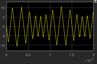
This plot shows the voltage waveform. As the resistance of the Variable Resistor block increases, the amplitude of the output waveform increases and the frequency decreases.
Triangle Waveform Voltage
See Also
Topics
- Model Triangle Wave Generator Using Operational Amplifiers
- Essential Steps for Constructing a Physical Model
- Parameterizing Blocks from Data Sheets