Modeling of via array with open signal vias
This example shows modeling of a via array containing open signal vias [1]. Variation of pitch (distance of the via array grid) and variation in the number of board layers is studied.
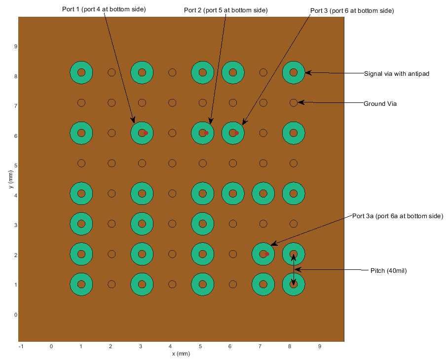
One Layer Simulations of Via Arrays
First, we simulate a one layer array, i.e., metal-dielectric-metal structure. The metal layers are made of Copper with a thickness of 3 mils. The dielectric layer has a thickness of 12 mils, permittivity of 3.7, and loss tangent of 0.03. The signal via has a via radius of 5 mils and an antipad radius of 15 mils.
Now, setup the viaSingleEnded object with corresponding properties:
obj = viaSingleEnded(SignalLayer = [1 3], GroundLayer = [1 3]);
obj.Conductor = metal('Name','Copper','Thickness',3*obj.mils2meters,'Conductivity',10e9);
obj.Substrate = dielectric('EpsilonR',3.7,'LossTangent',0.03,'Thickness',12*obj.mils2meters);
obj.SignalViaDiameter = 10*obj.mils2meters;
obj.SignalViaPad.Radius = 1.00001*obj.SignalViaDiameter/2;
obj.SignalViaAntipad.Radius = 15*obj.mils2meters;
Set up a grid containing the via locations
[X,Y] = meshgrid(1:8,1:8);
allXYs = [X(:) Y(:)];
Signal via locations:
[X,Y] = meshgrid([1 3 5 8],[1 2 4 6 8]);
SVXYs = [[X(:) Y(:)];7 1;7 2;7 4;1 3;3 3;5 3;6 4;6 6;6 8];
Ground via locations:
GRVXYs = setdiff(allXYs,SVXYs,'rows');Optionally, visualize the grid using:
plot(SVXYs(:,1),SVXYs(:,2),'r*')
hold on
plot(GRVXYs(:,1),GRVXYs(:,2),'b*')
legend('Signal vias','Ground return vias')
Detailed Study for 40 mil Pitch
pitch_var = 40; % in milsSet Signal via and Ground return via locations with a pitch of 40 mils:
obj.SignalViaLocations = [SVXYs*obj.mils2meters*pitch_var ...
    repmat([1 3],size(SVXYs,1),1)];
obj.GroundReturnViaLocations = [GRVXYs*obj.mils2meters*pitch_var ...
    repmat([1 3],size(GRVXYs,1),1)];
Define port locations for the signal vias:
Port 1 and Port 4 are at SV#9
Port 2 and Port 5 are at SV#14
Port 3 and Port 6 are at SV#28
Port 3a and Port 6a are at SV#22
The signal vias without ports defined are treated to be open.
obj.SignalTable = {9 1 0 "Vertical";...
    14 1 0 "Vertical";...
    28 1 0 "Vertical";...
    9 3 0 "Vertical"; ...
    14 3 0 "Vertical";...
    28 3 0 "Vertical";...
    22 1 0 "Vertical";...
    22 3 0 "Vertical"};
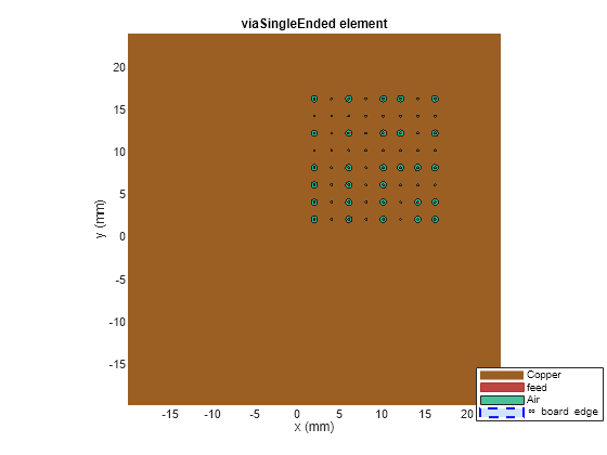
Visualize the 8x8 via array:
show(obj)
view(0,90)
zoom(1.6)
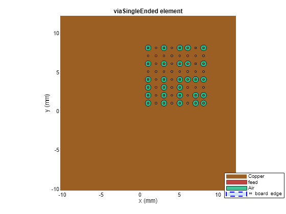
Compute the S-parameters of the board for frequencies up to 50 GHz.
NumPoints = 101;
freq = linspace(100e3,50e9,NumPoints);
spar_40mil = sparameters(obj,freq,"Behavioral",true);
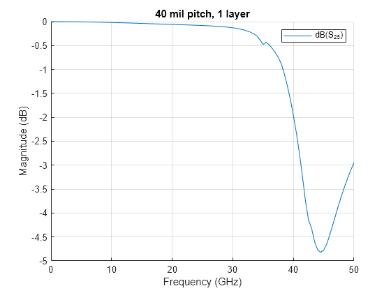
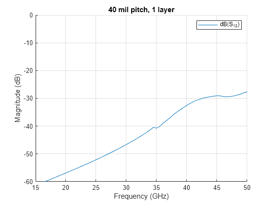
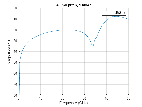
Plot S25, S12, and S22 and compare with results from [1]:
S25:
figure, hold on
setrfplot("engunits",false)
rfplot(spar_40mil,2,5)
title(pitch_var +" mil pitch, 1 layer")
S12:
figure, hold on
rfplot(spar_40mil,1,2)
title(pitch_var +" mil pitch, 1 layer")
ylim([-60 0])
S22:
figure, hold on
rfplot(spar_40mil,2,2)
title(pitch_var +" mil pitch, 1 layer")
ylim([-80 0])
Detailed Study for 80 mil Pitch
pitch_var = 80; % in milsUpdate Signal via and Ground return via locations with a pitch of 80 mils:
obj.SignalViaLocations = [SVXYs*obj.mils2meters*pitch_var ...
    repmat([1 3],size(SVXYs,1),1)];
obj.GroundReturnViaLocations = [GRVXYs*obj.mils2meters*pitch_var ...
    repmat([1 3],size(GRVXYs,1),1)];
Visualize the 8x8 via array:
show(obj)
view(0,90)
zoom(1.6)
Compute the S-parameters of the board for frequencies up to 50 GHz.
freq = linspace(100e3,50e9,NumPoints);
spar_80mil = sparameters(obj,freq,"Behavioral",true);
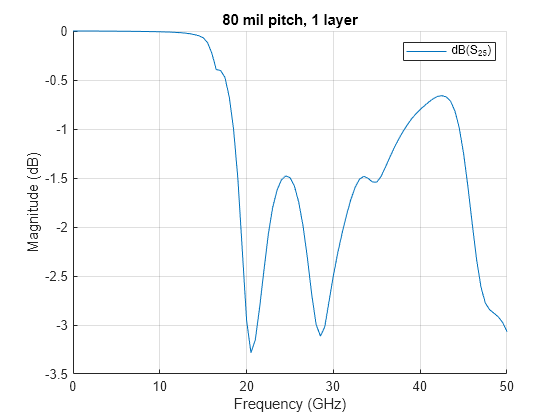
Plot S25:
figure, hold on
rfplot(spar_80mil,2,5)
title(pitch_var +" mil pitch, 1 layer")
Multilayer Simulations of Via Arrays
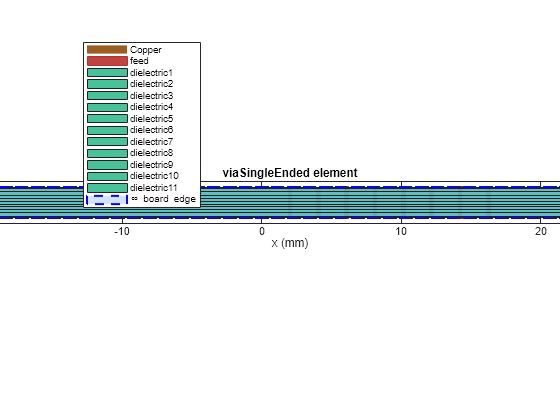
Analyze the same configuration of via arrays with 11 dielectric layers defined by d1 through d10. The corresponding metal layers have been defined by m1 through m12.
obj.SignalLayer = [1 23];
obj.GroundLayer = 1:2:23;
d1 = dielectric('EpsilonR',3.7,'LossTangent',0.03,'Thickness',3.8*obj.mils2meters);
d2 = dielectric('EpsilonR',3.7,'LossTangent',0.03,'Thickness',9.22*obj.mils2meters);
d3 = dielectric('EpsilonR',3.7,'LossTangent',0.03,'Thickness',9.84*obj.mils2meters);
d4 = dielectric('EpsilonR',3.7,'LossTangent',0.03,'Thickness',9.84*obj.mils2meters);
d5 = dielectric('EpsilonR',3.7,'LossTangent',0.03,'Thickness',6.58*obj.mils2meters);
d6 = dielectric('EpsilonR',3.7,'LossTangent',0.03,'Thickness',7.86*obj.mils2meters);
d7 = dielectric('EpsilonR',3.7,'LossTangent',0.03,'Thickness',6.64*obj.mils2meters);
d8 = dielectric('EpsilonR',3.7,'LossTangent',0.03,'Thickness',9.34*obj.mils2meters);
d9 = dielectric('EpsilonR',3.7,'LossTangent',0.03,'Thickness',9.36*obj.mils2meters);
d10 = dielectric('EpsilonR',3.7,'LossTangent',0.03,'Thickness',9.64*obj.mils2meters);
d11 = dielectric('EpsilonR',3.7,'LossTangent',0.03,'Thickness',3.66*obj.mils2meters);
obj.Substrate = [d1 d2 d3 d4 d5 d6 d7 d8 d9 d10 d11];
m1 = metal("Copper"); m1.Thickness = 2.4*obj.mils2meters;
m2 = metal("Copper"); m2.Thickness = 1.46*obj.mils2meters;
m3 = metal("Copper"); m3.Thickness = 1.42*obj.mils2meters;
m4 = metal("Copper"); m4.Thickness = 1.24*obj.mils2meters;
m5 = metal("Copper"); m5.Thickness = 1.36*obj.mils2meters;
m6 = metal("Copper"); m6.Thickness = 1.54*obj.mils2meters;
m7 = metal("Copper"); m7.Thickness = 1.36*obj.mils2meters;
m8 = metal("Copper"); m8.Thickness = 1.4*obj.mils2meters;
m9 = metal("Copper"); m9.Thickness = 1.3*obj.mils2meters;
m10 = metal("Copper"); m10.Thickness = 1.4*obj.mils2meters;
m11 = metal("Copper"); m11.Thickness = 1.4*obj.mils2meters;
m12 = metal("Copper"); m12.Thickness = 2.94*obj.mils2meters;
obj.Conductor = [m1 m2 m3 m4 m5 m6 m7 m8 m9 m10 m11 m12];
Define port locations for the signal vias:
obj.SignalTable = {9 1 0 "Vertical";...
    14 1 0 "Vertical";...
    28 1 0 "Vertical";...
    9 23 0 "Vertical"; ...
    14 23 0 "Vertical";...
    28 23 0 "Vertical";...
    22 1 0 "Vertical";...
    22 23 0 "Vertical"};
Update Signal via and Ground return via locations with a pitch of 80 mils and such that they are plated through hole (PTH) vias:
obj.SignalViaLocations = [SVXYs*obj.mils2meters*pitch_var ...
    repmat([1 23],size(SVXYs,1),1)];
obj.GroundReturnViaLocations = [GRVXYs*obj.mils2meters*pitch_var ...
    repmat([1 23],size(GRVXYs,1),1)];
Visualize the 8x8 via array:
show(obj)
view(0,0)
zoom(4)
legend('Location','northwest')
Compute the S-parameters of the board for frequencies up to 50 GHz.
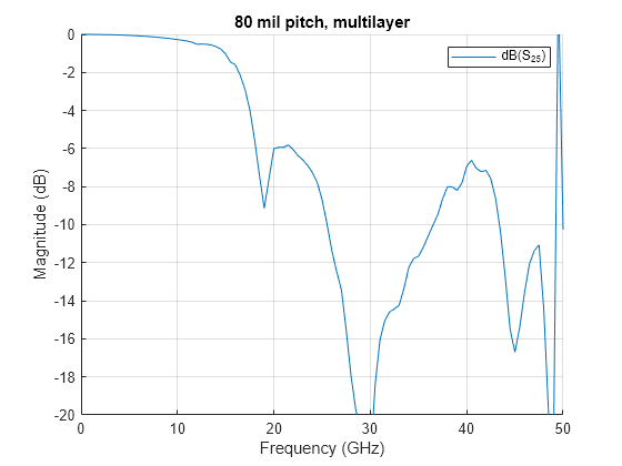
spar_40mil_multilayer = sparameters(obj,freq,"Behavioral",true);Plot S25, S22, S12, and S15:
S25:
figure, hold on
rfplot(spar_40mil_multilayer,2,5)
title(pitch_var +" mil pitch, multilayer")
ylim([-20 0])
S22:
figure
rfplot(spar_40mil_multilayer,2,2)
title(pitch_var +" mil pitch, multilayer")
ylim([-60 0])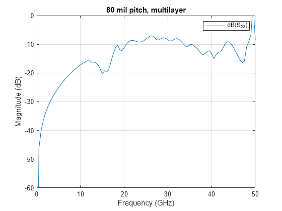
S12:
figure
rfplot(spar_40mil_multilayer,1,2)
title(pitch_var +" mil pitch, multilayer")
ylim([-60 0])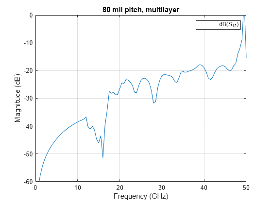
S15:
figure
rfplot(spar_40mil_multilayer,1,5)
title(pitch_var +" mil pitch, multilayer")
ylim([-60 0])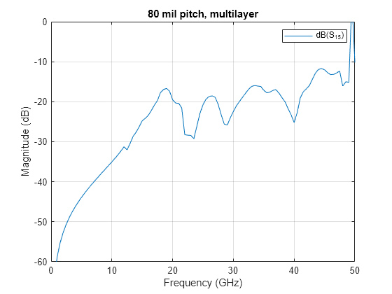
References
Sebastian Müller, "Via Array Modeling for Application in Fast, Energy-Efficient Digital Systems", Doctoral thesis, Technische Universität Hamburg, Germany, 2014. [Online]. Available: https://doi.org/10.15480/882.1219
Steinberger, Telian, Tsuk, Iyer and Yanamadala, “Proper Ground Via Placement for 40+ Gbps Signaling”, DesignCon 2022, April 2022.
Steinberger, Telian, Bell and Rowett, “Managing Differential Via Crosstalk and Ground Via Placement for 40+ Gbps Signaling”, DesignCon 2023, February 2023.
