Access FPGA Memory Using JTAG-Based AXI Manager
Use JTAG-based AXI manager to access the memories connected to the FPGA. In the FPGA, there is an AMD® DDR memory controller and BRAM controller exist for accessing the DDR memories and the BRAM, respectively. These memory controllers provide an AXI4 subordinate interface for write and read operations by other components in the FPGA. The JTAG-based AXI manager feature provides an AXI manager component that you can use to access any AXI subordinate IPs in the FPGA. This example demonstrates how to integrate AXI Manager IP into an AMD Vivado® project and how to write and read data from the DDR memory and the BRAM using MATLAB®. This example simulates the design using the Vivado simulator and then programs the FPGA and performs write and read operations from the MATLAB console.
Requirements
AMD Vivado Design Suite with supported version listed in FPGA Verification Requirements
Artix®-7 35T Arty FPGA Evaluation Kit
HDL Verifier™ Support Package for AMD FPGA and SoC Devices
JTAG cable
Setup
1. Set up the FPGA board. Connect the Arty board to the host computer via USB-JTAG cable.
2. Prepare the example in MATLAB. Set up the AMD Vivado tool path. Use your own AMD Vivado installation path when executing the command.
hdlsetuptoolpath('ToolName','Xilinx Vivado','ToolPath', ...
                 'C:\Xilinx\Vivado\2023.1\bin\vivado.bat');
Create a Vivado project for this example. This project contains the IP Integrator block diagram and constraint file for this example.
system('vivado -mode batch -source jtagAXIMcreateproject.tcl')
This command takes about one minute to run. When the execution completes, a Vivado project named arty.xpr appears in your current directory.
3. Configure the Vivado project with a Vivado IP. To use the AXI Manager IP inside the Vivado IP Integrator, add the folder that contains the IP to the Vivado IP repository path setting for the Vivado project. Add the path to the project by executing this command in MATLAB.
setupAXIManagerForVivado arty.xpr
Open the generated Vivado project in GUI mode by double-clicking the project in a file browser or executing this command in MATLAB.
system('vivado arty.xpr &')
4. Add AXI Manager IP to the FPGA design. In the Vivado GUI, open the block diagram design file jtagAXIMdesign_1.bd. You can find the design file in the source file subwindow.
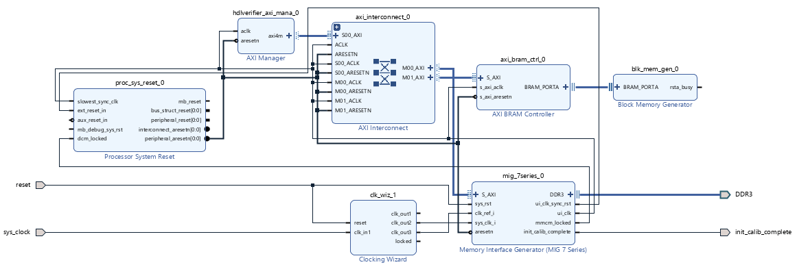
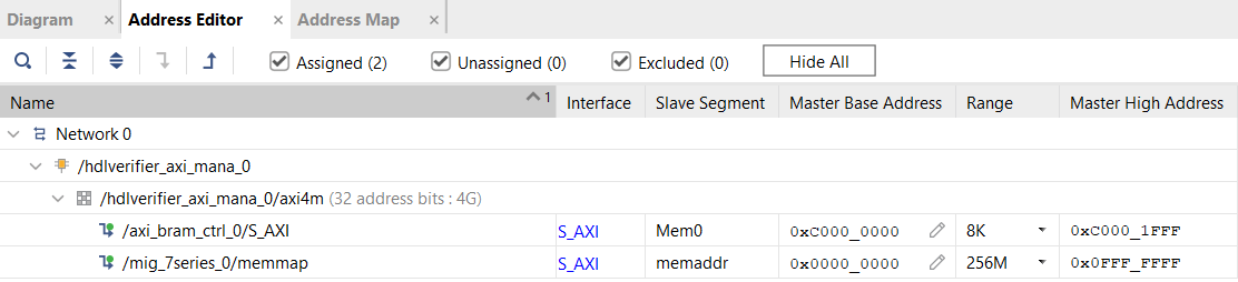
Set the address of mig_7series_0 (DDR controller) to 0x0000_0000 and axi_bram_ctrl_0 (BRAM controller) to 0xc000_0000 in the address editor as shown in this figure.
Alternatively, you can complete these steps by executing Tcl commands in Vivado.
source ./jtagAXIMmodifydesign.tcl
Write and Read Operations in Simulation
Click Run Simulation on the Vivado window to launch the simulation.
When simulation starts, the first few minutes are required to simulate the calibration process of the DDR3.
After the calibration, these lines in the jtagAXIMtestbench.sv file writes and reads 256 consecutive words (32-bit) of data from the address 0 using Increment mode.
wdata = new[256];
for(integer i =0;i<256;i=i+1)
wdata[i] = i+1;
wrapper.jtagAXIMdesign_1_i.hdlverifier_axi_mana_0.inst.writememory ...
 (0,wdata,hdlverifier::HDLV_AXI_BURST_TYPE_INCR);
wrapper.jtagAXIMdesign_1_i.hdlverifier_axi_mana_0.inst.readmemory ...
 (0,256,hdlverifier::HDLV_AXI_BURST_TYPE_INCR,rdata);
These commands write and read 256 consecutive word of data from the address 0xc000_0000 using Increment mode.
wdata = new[256];
for(integer i =0;i<256;i=i+1)
wdata[i] = i+1;
wrapper.jtagAXIMdesign_1_i.hdlverifier_axi_mana_0.inst.writememory ...
 (3221225472,wdata,hdlverifier::HDLV_AXI_BURST_TYPE_INCR);
wrapper.jtagAXIMdesign_1_i.hdlverifier_axi_mana_0.inst.readmemory ...
 (3221225472,256,hdlverifier::HDLV_AXI_BURST_TYPE_INCR,rdata);
Similarly, these lines show how to write a single word of value 100 into memory at address 0 and read it back.
wdata = new[1];
wdata[0] = 100;
wrapper.jtagAXIMdesign_1_i.hdlverifier_axi_mana_0.inst.writememory ...
 (0,wdata,hdlverifier::HDLV_AXI_BURST_TYPE_FIXED);
wrapper.jtagAXIMdesign_1_i.hdlverifier_axi_mana_0.inst.readmemory ...
 (0,1,hdlverifier::HDLV_AXI_BURST_TYPE_FIXED,rdata);
Generate FPGA Bitstream and Program FPGA
Click Generate Bitstream on the Vivado window to generate the FPGA programming file. Vivado might prompt you to save the project before proceeding to the next step. Generating the bitstream file takes about 5 to 10 minutes for Vivado to generate the bitstream file.
After Vivado generates the bitstream, program the FPGA by executing this command in MATLAB.
filProgramFPGA('AMD Vivado','arty.runs\impl_1\design_1.bit',1)
Write and Read Operations to FPGA
After programming the FPGA, you can write and read from the AXI subordinates connected to the AXI Manager IP. This example writes data to the DDR memory connected to the FPGA and the BRAM and then retrieves data into MATLAB.
Create the AXI manager object in MATLAB to write and read from the DDR memory. Write single location and then read data from the same location. In this case, the read data is 100.
h = aximanager('AMD');
writememory(h,'00000000',100);
readmemory(h,'00000000',1);
Use any address in the range form c000_0000 to c000_1FFF to write and read from the BRAM. Write single location and then read data from the same location. In this case, the read data is 1000.
writememory(h,'c0000000',1000);
readmemory(h,'c0000000',1);
See Also
aximanager | writememory | readmemory