FPGA Board Customization
Feature Description
Both HDL Coder™ and HDL Verifier™ software include a set of predefined FPGA boards you can use with the FPGA-in-the-loop (FIL) workflow. You can view the lists of these supported boards in the HDL Workflow Advisor or in the FIL wizard. With the FPGA Board Manager, you can add additional boards to use either of these workflows. To add a board, you need the relevant information from the board specification documentation.
The FPGA Board Manager is the hub for accessing wizards and dialog boxes that take you through the steps necessary to create a custom board configuration. You can also access options for:
Importing a custom board
Copying a board definition file for further modification
Verifying a new board
Custom Board Management
You manage FPGA custom boards through the following user interfaces:
FPGA Board Manager: portal to adding, importing, deleting, and otherwise managing board definition files.
New FPGA Board Wizard: This wizard guides you through creating a custom board definition file with information you obtain from the board specification documentation.
FPGA Board Editor: user interface for viewing or editing board information.
To begin, review the FPGA Board Requirements and then follow the steps described in Create Custom FPGA Board Definition.
FPGA Board Requirements
FPGA Device
To view a current list of supported FPGA device families with FPGA-in-the-loop (FIL), see Supported FPGA Device Families for Board Customization (HDL Verifier).
FPGA Design Software
Altera® Quartus® II or AMD® ISE is required. See product documentation for HDL Coder or HDL Verifier for the specific software versions required.
The following MathWorks® tools are required to use FIL.
| Workflow | Required Tools |
|---|---|
| FPGA-in-the-loop |
|
General Hardware Requirements
To use an FPGA development board, make sure that you have the following FPGA resources:
Clock: An external clock connected to the FPGA is required. The clock can be differential or single-ended. The accepted clock frequency is from 5 MHz to 300 MHz. When used with FIL, there are additional requirements to the clock frequency (see Ethernet Connection Requirements for FPGA-in-the-Loop).
Reset: An external reset signal connected to the FPGA is optional. When supplied, this signal functions as the global reset to the FPGA design.
JTAG download cable: A JTAG download cable that connects host computer and FPGA board is required for the FPGA programming. The FPGA must be programmable using AMD iMPACT or Altera Quartus II.
Ethernet Connection Requirements for FPGA-in-the-Loop
Supported Ethernet PHY Device. On the FPGA board, the Ethernet MAC is implemented in FPGA. An Ethernet PHY chip is required to be on the FPGA board to connect the physical medium to the Media Access (MAC) layer in the FPGA.
Note
When programming the FPGA, HDL Verifier assumes that there is only one download cable connected to the Host computer. It also assumes that the FPGA programming software automatically recognizes the cable. If not, use FPGA programming software to program your FPGA with the correct options.
The FIL feature is tested with the following Ethernet PHY chips and may not work with other Ethernet PHY devices.
| Ethernet PHY Chip | Test |
|---|---|
| Marvell® Alaska 88E1111 | For GMII, RGMII, SGMII, and 100 Base-T MII interfaces |
| National Semiconductor DP83848C | For 100 Base-T MII interface only |
Ethernet PHY Interface. The Ethernet PHY chip must be connected to the FPGA using one of the following interfaces:
| Interface | Note |
|---|---|
| Gigabit Media Independent Interface (GMII) | Only 1000 Mbits/s speed is supported using this interface. |
| Reduced Gigabit Media Independent Interface (RGMII) | Only 1000 Mbits/s speed is supported using this interface. |
| Serial Gigabit Media Independent Interface (SGMII) | Only 1000 Mbits/s speed is supported using this interface. |
| Media Independent Interface (MII) | Only 100 Mbits/s speed is supported using this interface. |
Note
For GMII, the TXCLK (clock signal for 10/100 Mbits signal) signal is not required because only 1000 Mbits/s speed is supported.
In addition to the standard GMII/RGMII/SGMII/MII interface signals, FPGA-in-the-loop also requires an Ethernet PHY chip reset signal (ETH_RESET_n). This active-low reset signal performs the PHY hardware reset by FPGA. It is active-low.
Special Timing Considerations for RGMII. When the RGMII interface is used, the MAC on the FPGA assumes that the data are aligned with the edges of reference clock as specified in the original RGMII v1.3 standard. In this case, PC board designs provide additional trace delay for clock signals.
The RGMII v2.0 standard allows the transmitter to integrate this delay so that PC board delay is not required. Marvell Alaska 88E1111 has internal registers to add internal delays to RX and TX clocks. The internal delays are not added by default, which means that you must use the MDIO module to configure Marvell 88E1111 to add internal delays. For more information on the MDIO module, see FIL I/O.
Special Clock Frequency Requirement for GMII/RGMII/SGMII Interface. When GMII/RGMII/SGMII interfaces are used, the FPGA requires an exact 125 MHz clock to drive the 1000 Mbits/s communication. This clock is derived from the user supplied external clock using the clock module or PLL.
Not all external clock frequencies can derive an exact 125 MHz clock frequency. The acceptable clock frequencies vary depending on the FPGA device family. The recommended clock frequencies are 50, 100, 125, and 200 MHz.
JTAG Connection Requirements for FPGA-in-the-Loop
| Vendor | Required Hardware | Required Software | JTAG Clock Frequency |
|---|---|---|---|
| Intel® | USB Blaster I or USB Blaster II download cable |
| 12 or 24 MHz |
| AMD | Digilent® download cable
|
| 33 MHz |
FTDI USB-JTAG cable
| Install these D2XX drivers:
For the installation guide, see D2XX Drivers from the FTDI Chip website. | 15 MHz | |
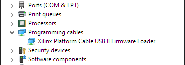
| Platform Cable USB II | Run the driver installer before you use the cable by following these steps:
For more information about driver installation, see Platform Cable USB II Data Sheet (DS593) from the AMD website. | 12 MHz | |
| Microchip | JTAG connection not supported | ||