Model Design for AXI4 Master Interface Generation
For designs that require accessing large data sets from an external memory, model your
algorithm with a simplified AXI4 Master protocol. When you
run the IP Core Generation workflow, HDL Coder™ generates an IP core with AXI4 Master
interfaces. The AXI4 Master interface can communicate
between your design and the external memory controller IP by using the AXI4
Master protocol. Use the AXI4
Master interface when your:
Design targets multi-frame video processing applications. You can store the image data in external memory, such as a DDR3 memory on board, and then read or write the images to your design in a burst fashion for high-speed processing.
Algorithm must access memory data in a non-streaming arbitrary pattern.
DUT IP core must control other IPs with the register interfaces, such as AXI4 and AXI4-Lite, in the system. This capability is especially useful in standalone FPGA devices.
Simplified AXI4 Master Protocol - Write Channel
To map the DUT ports to AXI4 Master interfaces, use
the simplified AXI4 Master protocol. You do not have to
model the actual AXI4 Master protocol. Instead, you can
use the simplified protocol. When you run the IP Core Generation
workflow, the generated HDL code contains wrapper logic that translates between the
simplified protocol and the actual AXI4 Master protocol.
The simplified protocol requires fewer protocol signals, eases the handshaking
mechanism between valid and ready signals, and supports bursts of arbitrary
lengths.
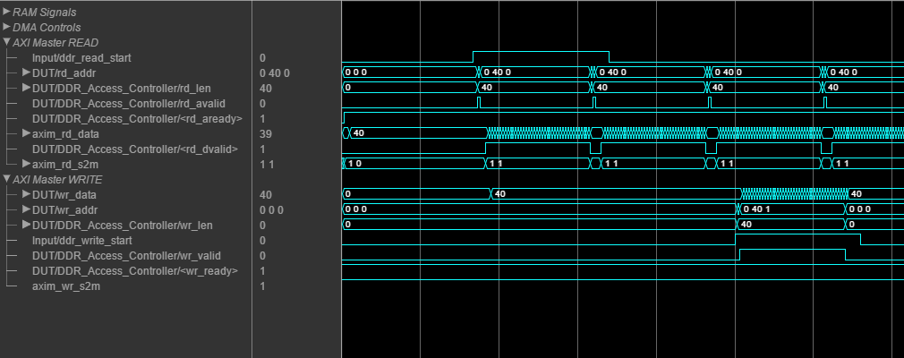
For a write transaction, use the simplified AXI4 Master write protocol. For a read transaction, use the simplified AXI4 Master read protocol. This figure shows the timing diagram for the signals that you model at the DUT input and output interfaces for an AXI4 Master write transaction.

The DUT waits for wr_ready to become high to initiate a write
request. When wr_ready becomes high, the DUT can send the write
request. The write request consists of the Data and
Write Master to
                    Slave bus
signals. This bus consists of
wr_len, wr_addr, and
wr_valid. The wr_addr signal specifies the
starting address that the DUT writes to. The wr_len signal
corresponds to the number of data elements in this write transaction.
Data can be sent when wr_valid is high.
When wr_ready becomes low, the DUT must stop sending data within
one clock cycle, and the Data signal becomes invalid. If the DUT
continues to send data after one clock cycle, the data is ignored.
The simplified AXI4 Master Protocol supports pipelined
requests. The protocol is not required to wait for the
wr_complete signal to be high before issuing a subsequent
write request. The interface supports up to 16 transactions (or 16 data words)
before the pipeline stalls and the wr_ready signal goes
low.
Output Signals
Model the Data and Write
Master to Slave
bus signals at the DUT output interface.
Data: The data that you want to transfer, valid each cycle of the transaction.Write Master to Slave busthat consists of:wr_addr: Starting address of the write transaction that is sampled at the first cycle of the transaction. The address is specified in bytes.wr_len: The number of data values that you want to transfer, sampled at the first cycle of the transaction. Thewr_lensignal is specified in words, meaning that each unit ofwr_lenis a complete data element. For example, whenwr_lenis2, and the bit width of data is128bit, two128-bit data elements are written.wr_valid: When this control signal becomes high, it indicates that theDatasignal sampled at the output is valid.wr_awid(optional signal): This signal is the address ID that identifies multiple streams over a single channel. When you do not mapwr_awid, the generated IP core setswr_awidto a constant 0.
Input Signals
Model the Write Slave to
Master bus that consists of:
wr_complete(optional signal): Control signal that when high for one clock cycle, indicates that the write transaction has completed. The next burst of data can be sent afterwr_completeasserts. The early assertion ofwr_completemakes the average latency nearly3clock cycles between two bursts, which makes the write operation pipelined and improves the write throughput.wr_ready: This signal corresponds to the back pressure from the slave IP core or external memory. When this control signal goes high, it indicates that data can be sent. Whenwr_readyis low, the DUT must stop sending data within one clock cycle. You can also use thewr_readysignal to determine whether the DUT can send a second burst signal immediately after the first burst signal has been sent. Multiple burst signals are supported, which means that thewr_readysignal remains high to accept the second burst immediately after the last element of the first burst has been accepted. Usingwr_readyto determine when to start the next burst can reduce the average latency between two bursts to less than3clock cycles.wr_bvalid(optional signal): Response signal from the slave IP core that you can use for diagnosis purposes. Thewr_bvalidsignal becomes high after the AXI4 interconnect accepts each burst transaction. Ifwr_lenis greater than256, the AXI4 Master write module splits the large burst signal into 256-sized bursts. Thewr_bvalidsignal becomes high for each 256-sized burst.wr_bresp(optional signal): Response signal from the slave IP core that you can use for diagnosis purposes. Use this signal with thewr_bvalidsignal.wr_bid(optional signal): This signal is the write response ID that identifies multiple streams over a single channel. When you do not mapwr_bid, the generated IP core terminateswr_bid.
The AXI4 Master protocol supports a maximum burst size
of 256. When you have a large burst size of greater than
256, the AXI Master interface in
the generated HDL IP core divides the large burst into multiple smaller bursts with
size 256. Even for large bursts of data, you see an improved
write throughput.
Simplified AXI4 Master Protocol - Read Channel
This figure shows the timing diagram for the signals that you model at the DUT
input and output interfaces for an AXI4 Master read
transaction. These signals include the Data, Read
Master to Slave
Bus, and Read Slave to
Master Bus.

The DUT waits for rd_aready to become high to initiate a read
request. When rd_aready is high, the DUT can send out the read
request. The read request consists of the rd_addr,
rd_len, and rd_avalid signals of the
Read Master to
                    Slave bus
. The
slave IP or the external memory responds to the read
request by sending the Data at each clock cycle. The
rd_len signal corresponds to the number of data values to
read. The DUT can receive Data as long as
rd_dvalid is high.
Read Request
To model a read request, at the DUT output interface, model the Read
Master to Slave
bus that consists of:
rd_addr: Starting address for the read transaction that is sampled at the first cycle of the transaction. The address is specified in bytes.rd_len: The number of data values that you want to read, sampled at the first cycle of the transaction. Therd_lensignal is specified in words, meaning each unit ofrd_lenis a complete data element. For example, whenrd_lenis2, and the bit width of data is128bit, two128-bit data elements are read.rd_avalid: Control signal that specifies whether the read request is valid.rd_arid(optional signal): This signal is the address ID that identifies multiple streams over a single channel. When you do not maprd_arid, the generated IP core setsrd_aridto a constant 0.
At the DUT input interface, you can model the ready signal
rd_aready to indicate when to send a new read request. The
rd_aready signal indicates whether the DUT can send consecutive
multiple burst requests. The DUT can send a new request one clock cycle after the
ready signal is asserted. After the ready signal is de-asserted, the DUT can send
one more read request. The DUT cannot send a new read request and the request is
ignored one clock cycle after the ready signal is de-asserted.
The simplified AXI4 Master Protocol supports pipelined
requests, so it is not required to wait for the read response to complete before
issuing a subsequent read request. The interface supports up to four read
transactions before the pipeline stalls and the rd_aready signal
goes low.
Read Response
At the DUT input interface, model the Data and Read
Slave to Master
bus signals.
Data: The data that is returned from the read request.Read Slave to Master busthat consists of:rd_dvalid: Control signal, which indicates that theDatareturned from the read request is valid.rd_rresp(optional signal): Response signal from the slave IP core that indicates the status of the read transaction.rd_rid(optional signal): This signal is the data ID that identifies multiple streams over a single channel. When you do not maprd_rid, the generated IP core terminatesrd_rid.
At the DUT output interface, you can optionally implement the
rd_dready signal. This signal is part of the Read
Master to Slave
bus and indicates when the DUT can start accepting data. By default,
if you do not map this signal to the AXI4 Master read
interface, the generated HDL IP core ties the rd_dready signal to
logic high.
Base Address Register Calculation
For IP cores that you generate, HDL Coder includes a base address register to support driver authoring for both
the AXI4 Master read and write channels. The base
address register is added to the address that is specified by the DUT
ADDR port to form the AXI4 Master address.
This capability enables the driver to use an addressing mode that programs a fixed
register address with the base address of a buffer. The programmed address together
with the DUT ADDR port is used to index the buffer. By default,
the registers take a value of zero, if you do not use them.

Specify Initial Value of AXI4 Master Read and Write Base Address
When you run the IP Core Generation workflow or the
Simulink Real-Time FPGA I/O workflow, you can specify an
initial value for the AXI4 master data read and write
base address registers. By default, the initial value is zero. To specify a nonzero value:
In the target platform interface table, when you map an input DUT port to an AXI4 Master Read data port, or an output DUT port to an AXI4 Master Write data port interface, an Options button appears in the Interface Options column.
Click the Options button, and then specify the DefaultReadBaseAddress or DefaultWriteBaseAddress.
Modeling for AXI4 Master Interfaces
You can model your algorithm with Data and AXI4 Master protocol signals at the DUT ports and then map the signals to AXI4 Master interfaces.

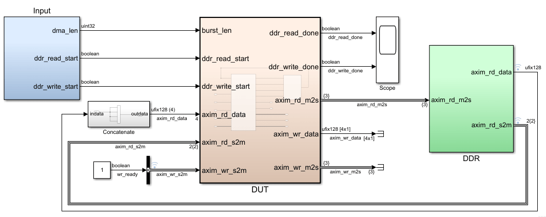
To learn how to model your DUT algorithm for AXI4 Master interface mapping, open this Simulink® model. The DUT subsystem contains a simple algorithm that reads data from the DDR and writes the data back to a different address in the DDR memory.
open_system('hdlcoder_axi_master')
sim ('hdlcoder_axi_master')
Open the DUT subsystem. The DDR_Access_Controller subsystem models the AXI Master read and write channels and has a Simple Dual Port RAM block that calculates the wr_data signal. If you double-click the DDR_Access_Controller subsystem, you see two edge detection Subsystem blocks that generate the two start pulses as input to each MATLAB Function block. One edge detection subsystem and DDR Read Controller MATLAB Function block models the read transaction. The other edge detection subsystem and DDR Write Controller MATLAB Function block models the write transaction. You can modify this design to model only the write transaction or the read transaction by using one edge detection subsystem and the corresponding MATLAB Function block.
Read Channel
The DDR Read Controller is modeled as a state machine with four states: INIT, IDLE, READ_BURST_START, and DATA_COUNT. The INIT state initializes the read signals and the RAM input signals. When the start signal becomes high, the state machine switches to the IDLE state, and then waits for the rd``_a``ready signal to become high. When rd``_a``ready becomes high, the state machine transitions to the READ_BURST_START state and the DUT starts reading data. The state machine then unconditionally switches to the DATA_COUNT state and continues to read data till rd``_a``valid goes low.
Write Channel
The DDR Write Controller is modeled similar to the Read channel as a state machine with four states: IDLE, WRITE_BURST_START, DATA_COUNT, and ACK_WAIT. The DUT is in the IDLE state and then switches to the WRITE_BURST_START state where it waits for the wr``_r``eady signal. When wr``_r``eady becomes high, the state machine switches to the DATA_COUNT state and starts writing data. The data is valid when wr``_v``alid is high. The DUT continues to write data when wr``_r``eady is high. As wr``_r``eady becomes low, the state machine switches to the ACK_WAIT state and then waits for the ready signal to initiate the next write transaction.
To see the simplified AXI4 Master protocol in effect, simulate the model. If you have DSP System Toolbox™ installed, you can view and analyze the results in the Logic Analyzer.
You can use the IP Core Generation workflow to generate an HDL IP core with the AXI4 Master interface. If you have HDL Verifier™ installed, and you use the Xilinx® Zynq® ZC706 board, then you can integrate the IP core into the Default System with External DDR3 memory access reference design.
Map Vector Ports to AXI4 Master Interfaces
When you map vector ports to the AXI4 Master interface, HDL Coder concatenates all elements of the vector to their combined bit width in the generated code. For example, a 4-element vector of the 128-bits vector is concatenated into 512-bits data in the generated code. The AXI4 Master interface supports a maximum bit width of 1024 bits. If your vector port has a combined bit width that exceeds 1024 bits, you get an error.
Note
Before R2024b, Simulink® supported fixed-point data types with word lengths up to 128 bits. As a result, you achieved bit widths greater than 128 bits in the generated code by using vector data types. Starting R2024b, you can directly model fixed-point data types with a bit width greater than 128 bits in Simulink and generate code. Using larger bit widths helps achieve higher throughput when accessing external DDR memory or fulfill requirements when integrating your HDL IP core into existing designs.
For example, in the
hdlcoder_axi_master model, to
expand the bit width of the axim_rd_data port to 512 bits,
specify a data type with the desired word length. Alternatively, to achieve a
512-bit width using vector concatenation, change the ddr_data
parameter inside the DDR to fi(([40:-1:1]),0,128,0) and then
concatenate the 128-bit input four times. This method generates an output of 512
bits using a Vector Concatenate block. To simulate the model, replace
the Simple Dual Port RAM block inside the DUT subsystem with a
Simple Dual port RAM System block.
You can then map these DUT Data ports to AXI4
Master Read or AXI
Master Write ports in the Target
platform interface table, generate the HDL IP core, and integrate the IP core into
your Vivado® or Qsys reference designs. In the generated HDL code for the DUT IP
core, the Data ports are mapped to 512-bit
interfaces. Multiple FIFO blocks are generated corresponding to each element of the
vector input.
ENTITY DUT_ip IS
PORT( IPCORE_CLK : IN std_logic; -- ufix1
IPCORE_RESETN : IN std_logic; -- ufix1
AXI4_Master_Rd_RDATA : IN std_logic_vector(511 DOWNTO 0); -- ufix256
...
...
AXI4_Master_Wr_WDATA : OUT std_logic_vector(511 DOWNTO 0); -- ufix256
...
);
END DUT_ip;This figure illustrates the order in which the vector data is written to and read form.

In the HDL code for the DUT IP core, you can see how the
AXI4_Master_Rd_RDATA and
AXI4_master_Wr_WDATA interfaces
are mapped to the DUT ports and the order in which data is written to the AXI4
Master interface and then read back.
...
...
--------------------------------------------------------------------
AXI4 Master Read Sequence
--------------------------------------------------------------------
AXI4_Master_Rd_RDATA_0 <= AXI4_Master_Rd_RDATA_unsigned(127 DOWNTO 0);
AXI4_Master_Rd_RDATA_1 <= AXI4_Master_Rd_RDATA_unsigned_1(255 DOWNTO 128);
AXI4_Master_Rd_RDATA_2 <= AXI4_Master_Rd_RDATA_unsigned_7(383 DOWNTO 256);
AXI4_Master_Rd_RDATA_3 <= AXI4_Master_Rd_RDATA_unsigned_7(511 DOWNTO 384);
--------------------------------------------------------------------
AXI4 Master Write Sequence
--------------------------------------------------------------------
AXI4_Master_Wr_WDATA_tmp <= unsigned(AXI4_Master_Wr_WDATA_Vec_3) &
unsigned(AXI4_Master_Wr_WDATA_Vec_2) &
unsigned(AXI4_Master_Wr_WDATA_Vec_1) &
unsigned(AXI4_Master_Wr_WDATA_Vec_0);
AXI4_Master_Wr_WDATA <= std_logic_vector(AXI4_Master_Wr_WDATA_tmp);
...
...
If you use a nonstandard bit width for the AXI4 Master
Data port, the Data port is upgraded to a
standard bit width container that has a bigger size. Standard bit widths include
32, 64, 128,
256, 512, and 1024
bits. For example, if you use a vector that has four 35-bit
elements, the resulting bit width of 140 bits
(35x4) is mapped to a 256-bit AXI4
Master interface. At the Write channel
Data port, bits 255 to
141 are padded with zeroes. At the Read channel
Data port, bits 255 to
141 are ignored.

Using nonstandard bit widths can have a performance impact because the entire bandwidth of the AXI4 Master interface is not used. To avoid performance hits, use standard AXI bit widths.
Model ID Signals to Reduce the Number of AXI4 Master Interfaces
You can model ID signals for the Simplified AXI4 Master Protocol in the IP core generation workflow. Use ID signals to:
Allow multiple modules to share the same AXI Master Interface.
Enable out-of-order requests for data. ID signals allow an AXI Master to issue requests without waiting for a prior request to finish.
Reduce the amount of AXI4 Master Interfaces needed for a Simulink model.
You can model ID signals in a write channel by using the optional signals wr_awid and wr_bid. You can model ID signals in a read channel by using the optional signals rd_arid and rd_rid. ID signal widths have these limitations:
The ID widths must be an unsigned integer having a maximum of 32 bits.
The ID widths for the read and write channel of the same AXI4 Master interface must match. Different AXI Master interfaces can have different ID widths.
When there are multiple kernels in the DUT that want to access external memory, during IP core generation, you can generate the read and write AXI masters for each kernel interface inside the DUT. These AXI masters consume hardware resources and add critical delays to the entire IP core when the number of AXI masters increase.

To allow multiple modules to share the same AXI Master Interface to reduce hardware consumption and critical delays, you can use ID signals. Besides modeling the physical ID signals, model an arbitrator inside the DUT. Based on your design needs, the arbitrator can be extendable as the number of processing kernels increases.

To see the simple read arbitrator modeled in this design, open the multi_masters_with_ID.slx model and double-click the DUT subsystem.
Model Designs with Multiple Sample Rates
The HDL Coder software supports designs with multiple sample rates when you run the IP Core Generation workflow. When you map the interface ports to AXI4 Master interfaces, to use multiple sample rates, ensure that the DUT ports that map to these AXI4 interfaces run at the fastest rate of the design after HDL code generation.
To learn more, see Generate IP Core from Multirate Model.
Reference Designs for IP Core Integration
You can integrate the generated HDL IP core with AXI4 Master interfaces into these HDL Coder reference designs:
Default System with External DDR3 Memory Access: When your target platform isXilinx Zynq ZC706 evaluation kit.Default System with External DDR4 Memory Access: When your target platform isIntel Arria10 SoC development kit.Default system with External LPDDR4 Memory Access: When your target platform isXilinx Versal AI Core Series VCK190 Evaluation Kit.
To use these reference designs, you must have HDL Verifier™ installed. This figure shows a high level block diagram of the reference design architecture.

In this architecture, the HDL DUT IP block corresponds to the
IP core that is generated from the IP Core Generation workflow.
Other blocks in the architecture represent the predefined reference design, that
consists of a MATLAB® based JTAG AXI Manager IP that is provided by HDL Verifier. After you run the FPGA design on the board, using the JTAG AXI
Manager IP, you can use the input data in MATLAB to initialize the onboard DDR3 external memory. The HDL DUT
IP core reads the input data from the external memory via the AXI4
Master interface. The IP core then performs the
algorithm computation and writes the result to DDR3 memory via the AXI4
Master interface. The JTAG AXI Manager IP can read the
result from DDR3 memory and then verify the result in MATLAB.
Using the addAXI4MasterInterface method of the
hdlcoder.ReferenceDesign class, you
can integrate the IP core with AXI4 Master Interface
into your own custom reference design.
Restrictions
Synthesis tool: Must be
Xilinx VivadoorAltera QUARTUS II.Xilinx ISEis not supported.Target workflow: Use the
IP Core
                            Generation
workflow. To run the workflow, open the HDL Workflow Advisor from your DUT algorithm in Simulink. MATLAB to HDL workflow is not supported.Processor/FPGA synchronization: Must be
Free runningmode.