Microstrip Bowtie Patch Antenna for Wireless Indoor Communications
R2026bThis example shows how to design, simulate, and analyze a wideband microstrip bowtie patch antenna (MBA) operating in the X-band for wireless indoor communications using Antenna Toolbox™. It also demonstrates the implementation of a coaxial probe feed for the pcbStack object, which enables realistic modeling of PCB-based antennas.
For conventional microstrip patch antennas, the major limitation is their narrow impedance bandwidth, typically ranging from 1% to 5%. The bowtie patch antenna overcomes this limitation through its tapered geometry, which supports multiple closely spaced resonant modes that produce wideband performance.
This example reproduces the antenna design presented in [1], where a three-section stepped impedance microstrip line feed network matches the MBA to a 50-ohm coaxial feed. The antenna is fabricated on a low-loss Taconic substrate and designed to resonate near 10.2 GHz. The reference paper reports a measured impedance bandwidth of 9.71%, which is nearly double that of a conventional rectangular patch on the same substrate.
Define Bowtie Patch Dimensions
The bowtie radiating element has three parameters: the half-length W, the slot width lS, and the flare height lH. According to [1], the resonant length of the bowtie antenna is approximately twice the dielectric wavelength at the design frequency. At 10.2 GHz on a Taconic substrate (epsilon_r = 2.2), the dielectric wavelength is approximately 20.2 mm.
lH = 26e-3;  % flare height
lS = 5e-3;   % slot width
l = 22e-3;   % bowtie half-length
Define Feed Matching Network Dimensions
The microstrip line feed network consists of three cascaded transmission line sections with widths w1, w2, w3 and lengths l1, l2, l3. This stepped impedance transformer provides a broadband match between the 50-ohm coaxial feed and the complex impedance of the bowtie radiating element. The optimized dimensions achieve < -10 dB across the desired X-band operating range.
w1 = 1.88e-3;
w2 = 1.10e-3;
w3 = 2.20e-3;

l1 = 3.70e-3;
l2 = 6.00e-3;
l3 = 4.90e-3;
Define Substrate
Define the substrate to support wideband antenna operation by selecting a low-loss, low-permittivity material. Use a Taconic substrate with a relative permittivity of 2.2, thickness of 0.79 mm, and loss tangent of 0.002.
substrate = dielectric(Name="taconic",EpsilonR=2.2,...
    Thickness=0.79e-3,LossTangent=0.002);
Create Bowtie Patch Geometry
Construct the bowtie shape by combining a central rectangular section with two triangular flare sections. Use the rectangular section of width ls to form the narrow throat of the bowtie, and taper the triangular sections outward to the half-length W to create the characteristic bowtie profile. To obtain a symmetric radiating structure, form the complete bowtie by mirroring the half-bowtie about the Y-axis.
% Create bowtie
rect1 = antenna.Rectangle(Length=l,Width=lS);
vert1 = [-l/2 lS/2; -l/2 lH/2; l/2 lS/2];
tri1 = antenna.Polygon(Vertices=vert1);
vert2 = [-l/2 -lS/2; -l/2 -lH/2; l/2 -lS/2];
tri2 = antenna.Polygon(Vertices=vert2);

bow1 = tri1 + rect1 + tri2;
bow1 = translate(bow1,[-l/2,0 0]);

bow2 = copy(bow1);
bow2 = mirrorY(bow2);
Bowtie = bow1 + bow2;
Create Feed Network Geometry
Build the three-section stepped impedance transformer feed network. Each section has a distinct characteristic impedance determined by its width. This multi-section design achieves broader impedance matching compared to a single quarter-wave transformer.
feed1 = antenna.Rectangle(Length=w3,Width=l3);
feed2 = antenna.Rectangle(Length=w2,Width=l2,Center=[0 (l3+l2)/2]);
feed3 = antenna.Rectangle(Length=w1,Width=l1,Center=[0 l2+(l3+l1)/2]);

Feed = feed1 + feed2 + feed3;
Feed = translate(Feed,[0, -(l1+l2+l3)+0.3e-3, 0]);

BowtieFinal = Bowtie + Feed;
Create PCB Stack with Coaxial Feed
Assemble the antenna as a multi-layer PCB stack using the pcbStack object. Construct the stack with three layers:
Top layer: Bowtie patch with stepped impedance feed network
Middle layer: Taconic dielectric substrate
Bottom layer: Ground plane with coaxial feed via
Define a coaxial feed using the CoaxialFeed object with circular pad and antipad geometries. Create clearance for the signal via by subtracting antipad from the ground plane, and connect the via to the microstrip feed line on the top layer using the pad. To maintain a 50‑ohm characteristic impedance, choose the pad and antipad radius.
boardShape = antenna.Rectangle(Length=3*l,Width=2*lH);
gnd = copy(boardShape);
pcbS = pcbStack;
pcbS.BoardShape = boardShape;
pcbS.BoardThickness = substrate.Thickness;
Create two circles: one to define a via shape at the feed site, and the other to define the via antipad shape.
padR = 0.5e-3;
antipadR = 2.16e-3;
Center = [0 -(l1+l2+l3+lS/2)+1e-3];
cPad = antenna.Circle(Center=Center, Radius=padR, NumPoints=16);
cAntipad = antenna.Circle(Center=Center, Radius=antipadR, NumPoints=16);
Punch out the antipad shape on the ground plane, and add back in the pad shape.
gnd = gnd - cAntipad + cPad;
pcbS.Layers = {BowtieFinal, substrate, gnd};
pcbS.FeedFormat = "FeedDefinitions";
Create the CoaxialFeed object using cPad and cAntipad as the shapes for the PadShape and AntipadShape properties.
f = CoaxialFeed(PadShape=cPad, AntipadShape=cAntipad, ...
    SignalLayers=1, GroundLayers=3);
pcbS.FeedDefinitions = f;
Visualize Antenna Structure
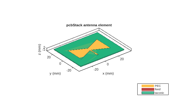
To verify the geometry, visualize the antenna structure by displaying the PCB stack. The top layer shows the bowtie patch with the three-section feed network, and the bottom layer shows the ground plane with the coaxial feed.
figure
show(pcbS)
Generate Mesh
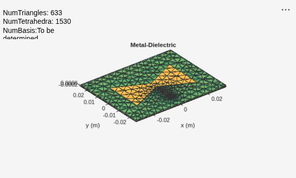
Mesh the antenna structure with a maximum edge length of 5 mm. This mesh density provides enough resolution for accurate analysis.
MaxEl = 5e-3;
figure
mesh(pcbS,MaxEdgeLength=MaxEl)
Compute S-Parameters
To capture the full resonant behavior of the antenna, calculate the S-parameters over the 8 GHz to 12 GHz frequency range. Use the response to evaluate the impedance matching performance and bandwidth of the MBA. The reference reports a measured dip at 10.2 GHz with additional dips observed at 9.86 GHz and 10.56 GHz, indicating the multi-resonant nature of the bowtie structure.
freqRange = linspace(8e9,12e9,1000);
sparam = sparameters(pcbS,freqRange,SweepOption="interp");
figure
rfplot(sparam)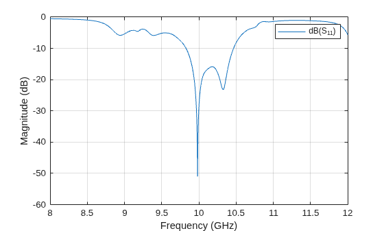
The simulated reflection coefficient shows two pronounced resonances, with reaching minimum values of approximately −47 dB at 9.98 GHz and −24 dB at 10.3 GHz. The shape of the simulated response is consistent with that reported in [1], showing similar dual-resonant behavior.
In particular, the dominant resonance near 9.98 GHz aligns closely with the reported dip around 9.94 GHz, while the second resonance at 10.3 GHz corresponds to the additional dips observed in the reference. Overall, the simulated response demonstrates strong agreement with the key characteristics of the measured and simulated results in [1], with closely aligned resonance locations and a similar profile.
Calculate Bandwidth
Determine the impedance bandwidth of the antenna defined as the frequency range over which < -10 dB (corresponding to VSWR < 2:1).
[~,~,flr,fup] = bandwidth(pcbS,freqRange,SweepOption="interp");
fl = flr(1);
fu = fup(1);
f_center = (fl + fu)/2;
BW_percent = (fu - fl)/f_center * 100;
fprintf("Bandwidth: %.2f%%\n",BW_percent)
Bandwidth: 6.29%
In the present simulation, the antenna achieves an impedance bandwidth of approximately 6.3%, which is higher than the bandwidth of a rectangular patch antenna, but still lower than the bandwidth reported in [1].
Plot Input Impedance
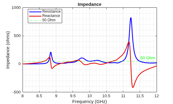
Visualize the input impedance variation over the operating frequency range. At the resonant frequency of 10.3 GHz, the antenna presents an impedance close to 50 ohms, confirming the effectiveness of the stepped impedance matching network.
figure; impedance(pcbS,freqRange,SweepOption="interp")
grid on;
grid minor;
yline(50, '--g', '50 Ohm');
l = legend;
l.String{end} = '50 Ohm';
Visualize Surface Current Distribution
Plot the surface current distribution on a logarithmic scale. The current distribution reveals how electromagnetic energy flows from the coaxial feed through the stepped impedance transformer and into the bowtie radiating element. High current density along the feed network confirms efficient power transfer to the radiator.
freq = 10.3e9;
figure; current(pcbS,10.2e9,Scale="log")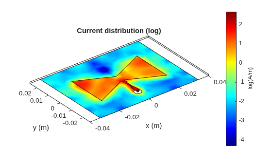
Compute E-Plane and H-Plane Radiation Patterns
Plot the elevation radiation patterns in the E-plane (phi = 0 degrees) and H-plane (phi = 90 degrees). The reference reports that at 10.2 GHz, the E-theta component exhibits a major dip in the broadside direction (θ = 0°) and a relatively minor dip around θ = ±45°, while the E-phi component has a slight dip at broadside. Both components are symmetric about the broadside axis, confirming well-behaved radiation characteristics.
figure;patternElevation(pcbS,freq)
title("E-Plane Radiation Pattern at 10.3 GHz")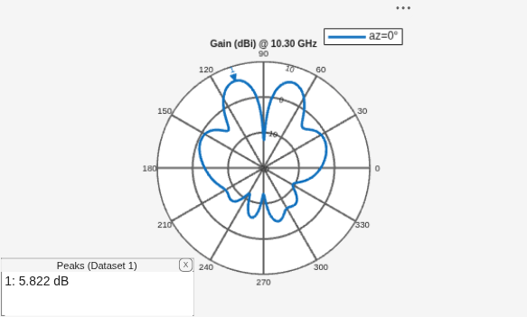
figure;patternElevation(pcbS,freq,90)
title("H-Plane Radiation Pattern at 10.3 GHz")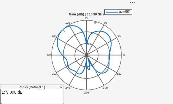
The simulated radiation pattern captures the overall shape characteristics of the antenna. In the E-plane, the variation between the main lobe and off-boresight directions is consistent with the expected behavior, particularly in the relative difference between the peak response and the level around 155°. This trend aligns well with the variations reported in the reference, indicating that the simulation reproduces the key directional characteristics of the antenna.
Conclusion
The simulation results show good agreement with the results reported in [1], successfully capturing the multi-resonant behavior of the bowtie antenna. While the reference reports a bandwidth of 9.71% centered at 10.2 GHz, the present simulation achieves approximately 6.3%, with resonance dips that shift slightly from the reference values. The radiation patterns exhibit the expected broadside symmetry in both E‑ and H‑planes, consistent with the reported trends. Overall, the results show reasonable agreement with the reference, validating the ability of the simulation to capture the key radiation and impedance matching characteristics of the antenna.
References
[1] Ng, C. H., S. Uysal, and M. S. Leong. “Microstrip Bowtie Patch Antenna for Wireless Indoor Communications.” Proceedings RAWCON 98. 1998 IEEE Radio and Wireless Conference (Cat. No.98EX194), 1998, 205–7. https://doi.org/10.1109/RAWCON.1998.709172.

