Memory Performance Information from FPGA Execution
Similar to the memory performance plots generated in simulation, you can collect memory interconnect traffic information from a design running on the FPGA. You can then generate similar performance plots. You can also capture the memory transaction information to view in the Logic Analyzer tool similar to the burst transactions from the memory controller in simulation. Use these plots to monitor real memory performance, debug and improve the design, and compare them against the memory performance obtained in simulation.
To include an AXI interconnect monitor (AIM) IP in your design, in the configuration parameters of the model, select the Include AXI interconnect monitor option under Hardware Implementation > Target hardware resources > FPGA design (debug). The AXI interconnect monitor IP collects information from the design while it is running on the FPGA. You can query this information from MATLAB® by using the JTAG connection. All memory masters in your FPGA are connected to the AXI interconnect monitor IP. These masters can include Memory Channel and Memory Traffic Generator blocks that you generated HDL code for or any other masters in your design.
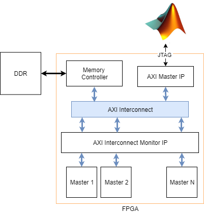
The SoC Builder tool generates a JTAG test bench script for your design. The script collects the performance metrics from the AXI interconnect monitor and launches the performance plot application, which plots the memory performance plots for bandwidth, number of bursts, and transaction latencies. These plots are similar to the plots of memory performance in simulation. You can also modify the script to collect and display memory transaction waveforms similar to the burst waveforms of memory controller in simulation. For information on the simulation memory performance, see Simulation Performance Plots and Buffer and Burst Waveforms.
For an example, see Analyze Memory Bandwidth Using Traffic Generators, which shows how to monitor memory performance in both simulation and when running on the FPGA. The script generated by the SoC Builder tool uses the JTAG connection to enable any traffic generators in your design, and then samples the memory performance information from the AXI interconnect monitor IP as fast as it can. The sampling interval depends on the JTAG latency, which is typically from 10 ms to 20 ms. The script then displays plots similar to the performance plots from the Memory Controller block in your simulation. The plot displays the bandwidth, number of bursts, and transaction latency for each master.
Note
The AXI manager itself is not connected to the AXI interconnect monitor. Therefore, the hardware diagnostics do not include the memory usage plots for test-bench-only masters that initialize the memory with predetermined data.
Memory Performance Plots
The script collects the performance metrics from the AXI interconnect monitor and launches the performance plot application.
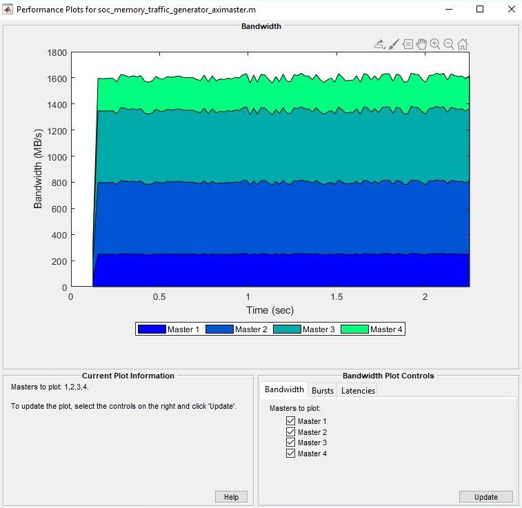
Memory Bandwidth Plots
In the Bandwidth tab, select the masters for which you want to graph bandwidth. Click Create Plot to see the bandwidth, in megabytes per second, for the selected masters over the duration of the run time. This figure shows the bandwidth for the Analyze Memory Bandwidth Using Traffic Generators example.
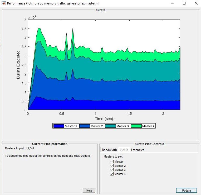
Memory Burst Plots
In the Bursts tab, select the masters for which you want to graph bursts. Click Create Plot to see the number of bursts executed for the selected master over the duration of the run time. This figure shows the burst count for the Analyze Memory Bandwidth Using Traffic Generators example.
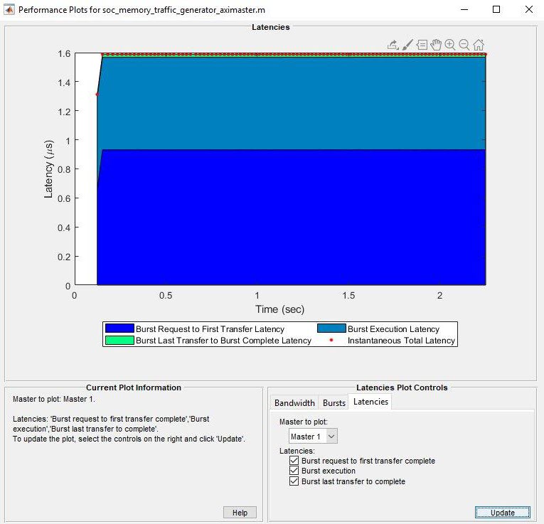
Memory Latency Plots
In the Latencies tab, select the
master for which you want to graph latencies. Click
Create Plot to see the latency, for the selected
masters over the duration of the run time. This image
shows the total latency for Master
1 in the Analyze Memory Bandwidth Using Traffic Generators example. You can then
zoom in to analyze the peak instantaneous latency.
You can choose from any of these options:
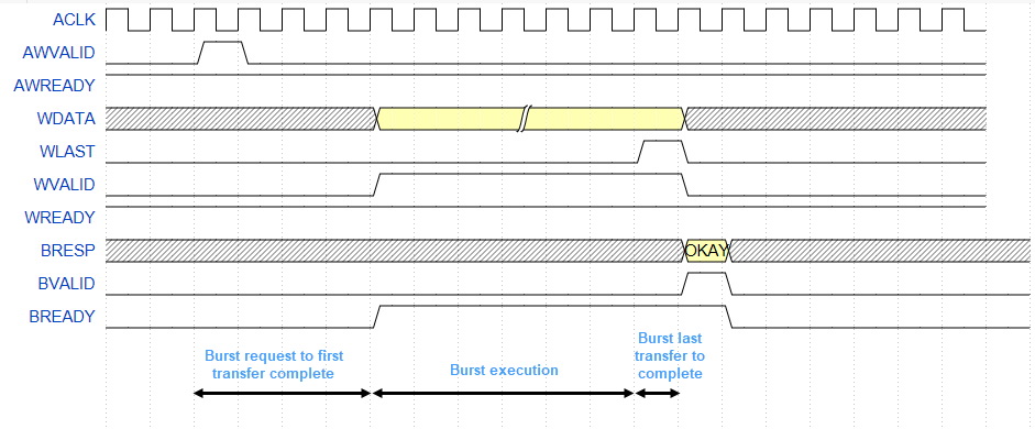
Burst request to first transfer complete — This option shows the time it takes from the moment the master issues a transaction request to the first transfer of data. This latency accounts for arbitration or interconnect delays.
Burst execution — This option shows the time it takes from the first transfer of data to the burst last transfer.
Burst last transfer to complete — This option shows the time it takes from last transfer to complete transaction. In case of read transaction, it is 0.
Instantaneous Total Latency — This option shows discrete total latency measurements per burst.
Each latency value plotted is an average of the respective latency, measured from the memory transactions over a sampling interval. The following figure shows an AXI4 Master protocol write and read transaction on the hardware showing each of these latencies.
Write Transaction
Read Transaction
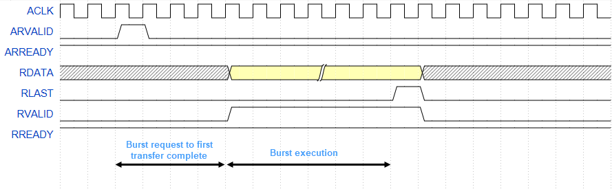
In read transaction, Burst last transfer to complete latency is zero.
Data Overflow
In Profile mode, the collectMemoryStatistics function samples memory metrics: bandwidth,
burst, and latencies values from the hardware after every sample. After that, the
function resets the metric counters and then starts the counters again for the next
sample. If any of the metric counters exceeds the limit of
232 — 1 within the sampling interval, the
counter is overflowed and the corresponding sample is indicated with
* in the plot.
Burst Waveforms
You can also modify the generated script to configure the AXI interconnect monitor to collect event data for each burst transaction. You can view these events in the Logic Analyzer waveform viewer to examine arbitration behavior. Specify the number of transactions to capture, Trace capture depth, in the configuration parameters of the model, under Hardware Implementation > Target hardware resources > FPGA design (debug).
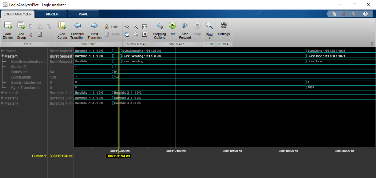
The waveforms show the event type (BurstIdle,
BurstRequest, BurstExecuting, or
BurstDone) and these parameters of the burst transaction:
MasterID–– ID number of the memory master that made the requestDataWidth–– Data width in bitsBurstLength–– Number of data words in the burst requestBurstsTransferred–– Number of bursts in this request (valid only withBurstDoneevent)BytesTransferred–– Number of bytes in this request (valid only withBurstDoneevent)
You can compare these waveforms with the waveforms captured from your Memory Controller block in simulation.
Configuring and Querying the AXI Interconnect Monitor
The AXI interconnect monitor (AIM) is an IP core that collects
performance metrics for an AXI-based FPGA design. Create an socIPCore
object to set up and configure the AIM IP, and use the socMemoryProfiler object to retrieve and display the data.
For an example of how to configure and query the AIM IP in your design using SoC AXI
Manager, see Analyze Memory Bandwidth Using Traffic Generators. Specifically, review the
soc_memory_traffic_generator_axi_master.m script that configures
and monitors the design on the device.
Select Memory Monitor Mode
The AXI interconnect monitor can collect two types of data. Choose
Profile mode to collect average transaction latency, and
counts of bytes and bursts. In this mode, you can open a performance plot tool, and
then configure the tool to plot bandwidth, burst count, and transaction latency.
Choose Trace mode to collect detailed memory transaction event
data and view the data as waveforms.
perfMonMode = 'Profile'; % or 'Trace'
Configure the AXI Interconnect Monitor
To
obtain diagnostic performance metrics from your generated FPGA design, you must set
up a JTAG connection to the device from MATLAB. Load a .mat file that contains structures derived
from the board configuration parameters. This file was generated by the SoC
Builder tool. These structures describe the memory interconnect and
masters configuration such as buffer sizes and addresses. Use the socHardwareBoard object to set up
the JTAG
connection.
load('soc_memory_traffic_generator_zc706_aximaster.mat');
hwObj = socHardwareBoard('Xilinx Zynq ZC706 evaluation kit','Connect',false);
AXIManagerObj = socAXIManager(hwObj);
socIPCore
object provides a function that performs this initialization. Next, set up a socMemoryProfiler object to gather the
metrics.apmCoreObj = socIPCore(AXIManagerObj,perf_mon,'PerformanceMonitor','Mode',perfMonMode); initialize(apmCoreObj); profilerObj = socMemoryProfiler(hwObj,apmCoreObj);
Retrieve Diagnostic Data
To retrieve performance metrics or signal data from a design running on the FPGA,
use the socMemoryProfiler object functions.
For Profile mode, call the collectMemoryStatistics function in a
loop.
NumRuns = 100;
for n = 1:NumRuns
    collectMemoryStatistics(profilerObj);
end
For Trace mode, call the collectMemoryStatistics function once. This function stops the IP
from writing transactions into the FIFO in the AXI interconnect
monitor IP, although the transactions continue on the interconnect. Set
the size of the transaction FIFO, Trace capture depth, in the
configuration parameters of the model, under Hardware Implementation > Target hardware resources > FPGA design (debug).
collectMemoryStatistics(profilerObj);
Visualizing Performance Metrics
Visualize the performance data using the plotMemoryStatistics function. In Profile mode,
this function opens a performance plot tool, and you can configure the tool to plot
bandwidth, burst count, and average transaction latency. In Trace
mode, this function opens the Logic Analyzer tool to view burst
transaction event
data.
plotMemoryStatistics(profilerObj);
See Also
Memory
Controller | socMemoryProfiler | collectMemoryStatistics | plotMemoryStatistics