Transmit Signal Waveform Using DDR4 on AMD RFSoC Device
This example shows how to design and implement a hardware algorithm on FPGA fabric using the IP core generation workflow. The algorithm writes test-signal waveform data to DDR4 memory, continuously reads the data using transmit repeat, and sends it to a digital-to-analog converter (DAC). The example also simulates the interaction between the hardware algorithm and external memory to verify behavior. After simulation, it generates HDL code for the algorithm as an IP core and integrates the core into a reference design to build a complete system. Finally, the example deploys the system to hardware and displays the received signal in Simulink®.
This example supports these hardware platforms:
AMD® Zynq® UltraScale+™ RFSoC ZCU111 evaluation kit and XM500 balun card
AMD Zynq UltraScale+ RFSoC ZCU216 evaluation kit and XM655 balun card
AMD Zynq UltraScale+ RFSoC ZCU208 evaluation kit and XM655 balun card
AMD Zynq UltraScale+ RFSoC DFE ZCU670 evaluation kit and XM755 balun card
Introduction
Using the IP core generation workflow, you can focus on the algorithm component and integrate it in a predefined reference design that defines the architecture. Use this workflow for rapid prototyping when a reference design that meets your system requirements is available for deployment.
Consider an RF application that requires high-speed waveform transmission. It often requires a memory subsystem capable of storing large data sets and delivering them at deterministic rates to a physical interface. DDR4 SDRAM provides the bandwidth and capacity needed for such applications, while Simulink offers a model-based design environment to prototype and validate the entire signal flow before hardware implementation. In this workflow, waveform samples are stored in DDR4 memory and repeatedly transmitted to a target interface, such as a DAC, using repeat logic. This approach is essential for applications like radar, wireless communication, and signal emulation, where continuous or cyclic waveform playback is required without CPU intervention.
In this example, MATLAB as a host sends a test signal waveform as workspace data to the PL DDR4 external memory. The hardware algorithm reads the DDR4 data continuously and sends it to the DAC channel of the RFSoC device. The signal waveform is then received from the analog-to-digital converter (ADC) channel in the FPGA. The receive-side FPGA uses logic to capture data and sends it to the host. Finally, the received data from memory is visualized by running the FPGA I/O script.
This example contains four models. All the models transmit a test signal waveform.
soc_waveform_tx_zcu111— Transmit a signal waveform on the ZCU111 board.
soc_waveform_tx_zcu216— Transmit a signal waveform on the ZCU216 board.
soc_waveform_tx_zcu208— Transmit a signal waveform on the ZCU208 board.
soc_waveform_tx_zcu670— Transmit a signal waveform on the ZCU670 board.
This example shows the workflow using the soc_waveform_tx_zcu111 model. The workflow steps are similar for all the models.
Workflow Setup
To work with the RFSoC support for a fixed reference design workflow, you must install and configure additional support packages and third-party tools. For more information, see AMD FPGA and SoC Devices.
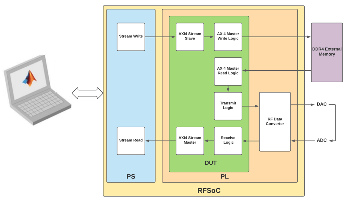
Model Structure
On the top level, this example model consists of RF Data Converter and AXI4 Random Access Memory blocks and Transmit and Repeat subsystem. On the transmit side, the Transmit and Repeat subsystem includes the Tx Transmit subsystem, which connects to the DAC in the RF Data Converter block. The Tx Transmit subsystem includes the DDR Transmit Repeat and the Tx NCO subsystems. The DDR Transmit Repeat subsystem reads waveform data from DDR4 and sends it to the DAC continuously using transmit repeat logic. In this example, the waveform data in DDR4 is a simple sine wave at 10 MHz. The Tx NCO subsystem generates two consecutive samples of the sinusoid waveform by using the NCO block. In the transmit path, either the DDR4 waveform or the sine wave generated by the NCO block is sent to the DAC based on the control input port txModeSel. By default, the DDR4 waveform is selected.
In the RF Data Converter block, the DAC interpolates the input data by a factor specified in the block mask. The DAC output loops back to the ADC in the RF Data Converter block. The ADC decimates the input data by a factor specified in the block mask. The ADC in the RF Data Converter block connects to the receive side of the Transmit and Repeat subsystem.
On the receive side, in the Transmit and Repeat subsystem, the Rx Capture subsystem writes the received data to internal BRAM using trigger and capture logic. You can use the input port FrameSize to specify the size of the data to read from BRAM. After that, it starts reading the data from BRAM and streams the data back to the host for further processing or display.
This example uses the IQ ADC/DAC Interface reference design to run on the Xilinx Zynq UltraScale+ RFSoC ZCU111 Evaluation Kit.
open_system('soc_waveform_tx_zcu111')
![]()
close_system('soc_waveform_tx_zcu111')
Simulate Model
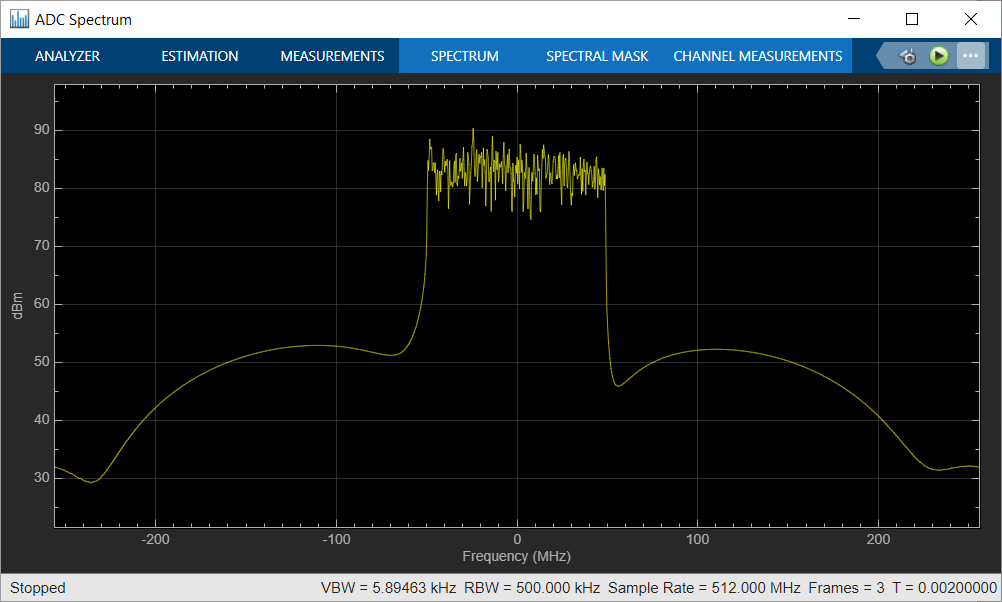
Simulate the model and observe the ADC captured signal waveform in the PlotData testbench subsystem for the transmitted signal waveform of 10 MHz signal.
Implement Algorithm
Hardware Setup for ZCU111 Kit
Connect the SMA connectors on the XM500 balun card to complete the loopback between the DACs and ADCs, according to the connections provided in the following table.

To implement the model on a supported SoC board, use the HDL Coder™ IP core generation workflow. To add the HDL Code tab to the Simulink toolstrip, open the Apps gallery and select HDL Coder.
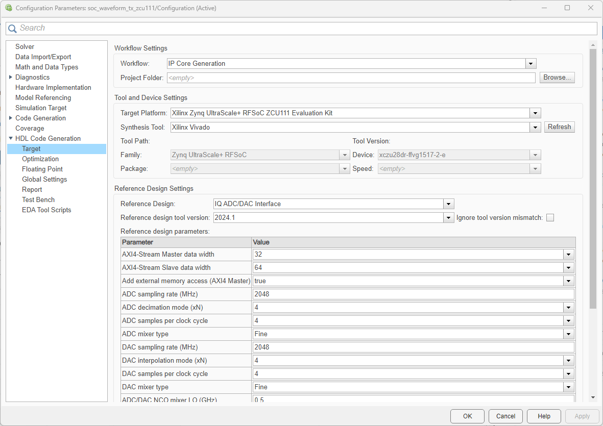
In the Configuration Parameters dialog box of the model, set the HDL workflow, target platform, and reference design by following these steps.
1. In the left pane, expand HDL Code Generation and then select Target.
2. Set Workflow to IP Core Generation.
3. Set Target Platform to Xilinx Zynq UltraScale+ RFSoC ZCU111 Evaluation Kit. Ensure that the Synthesis Tool is set to Xilinx Vivado.
4. Ensure that the Reference Design parameter is set to IQ ADC/DAC Interface.
5. Ensure that the AXI4-Stream Master data width parameter under Reference Design Settings is set to 32.
As the model includes the RF Data Converter block, the code generation process uses all the parameter values specified in the block. If model does not include this block, the process uses the reference design parameters for code generation.
To automatically map the interface of the IP, follow these steps.
1. Identify the IP core subsystem for code generation by selecting the Transmit and Repeat subsystem.
2. On the System on Chip tab, click Map Interfaces.

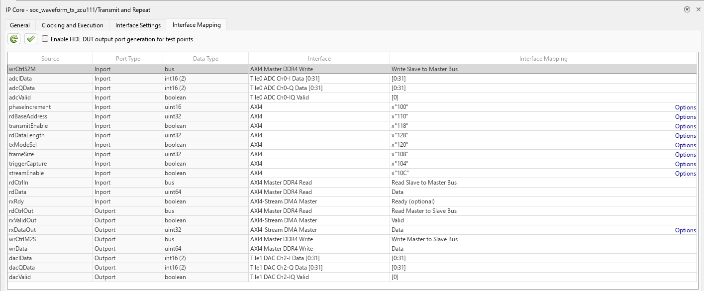
To view and edit the generated IP core interface mapping, follow these steps.
1. On the HDL Code toolstrip tab, click Target Interface.
2. In the IP Core panel, on the Interface Mapping tab, click the refresh button to load the mapping.
3. Edit the mapping until you map each DUT port and the mapping table appears as shown below.
4. Click the check button to validate the mapping.

Generate the HDL IP core and the FPGA bitstream files by following these steps.
1. On the HDL Code tab, click Build Bitstream.
2. After the HDL IP core generation finishes, an external shell opens for FPGA synthesis. Wait for the synthesis to complete. The FPGA synthesis often takes more than 30 minutes to complete.
For more information about the IP core generation workflow, see Get Started with IP Core Generation from Simulink Model (HDL Coder).
Run on Hardware
Program the FPGA on the SoC board by following these steps.
1. To download the bitstream, in the Simulink Toolstrip, on the HDL Code tab, select Build Bitstream > Program Target Device.
2. Verify your generated IP core on the hardware by using the generated host interface script. This script contains MATLAB commands that connect your hardware and interact with your IP core. To generate a host interface script file, in the Simulink Toolstrip, in the HDL Code tab, select Host Interface Script > Host Interface Script.
3. After downloading the bitstream, run the soc_waveform_tx_zcu111_io.m script (modified version of the generated host interface script) in the example folder to get the data back to the host from the hardware.
Implement and Run on ZCU216, ZCU208, and ZCU670
To generate the IP core and run the models soc_waveform_tx_zcu216, soc_waveform_tx_zcu208, and soc_waveform_tx_zcu670 on the hardware, follow the steps in the previous sections of this example and use the hardware setup as described in this section for connections.
Connect the SMA connectors on the XM655 balun card to complete the loopback between the DACs and ADCs of ZCU216 and ZCU208, and on the XM755 balun card to complete the loopback between the DACs and ADCs of ZCU670, according to the connections provided in the following table.
Hardware Setup for ZCU216, ZCU208, and ZCU670 Kits

Conclusion
Implement an algorithm that writes and reads the test waveform signal data into PL DDR4 memory and sends data continuously to DAC for transmission. Loop back the transmitted signal to the ADC and receive it back into the FPGA on an RFSoC device. Verify that the system works as expected on the hardware. You can use this example as a reference and prototype for your wireless algorithm to send any waveform signal on the AMD Zynq UltraScale+ RFSoC evaluation kits.