Design and Evaluate Successive Approximation ADC Using Stateflow
This example shows a 12-bit Successive Approximation Register (SAR) ADC with a circuit-level DAC model.
Successive Approximation ADCs typically have 12 to 16-bit resolution, and their sampling rates range from 10 kSamples/sec to 10 MSamples/sec. They tend to cost less and draw less power than subranging ADCs.
Model
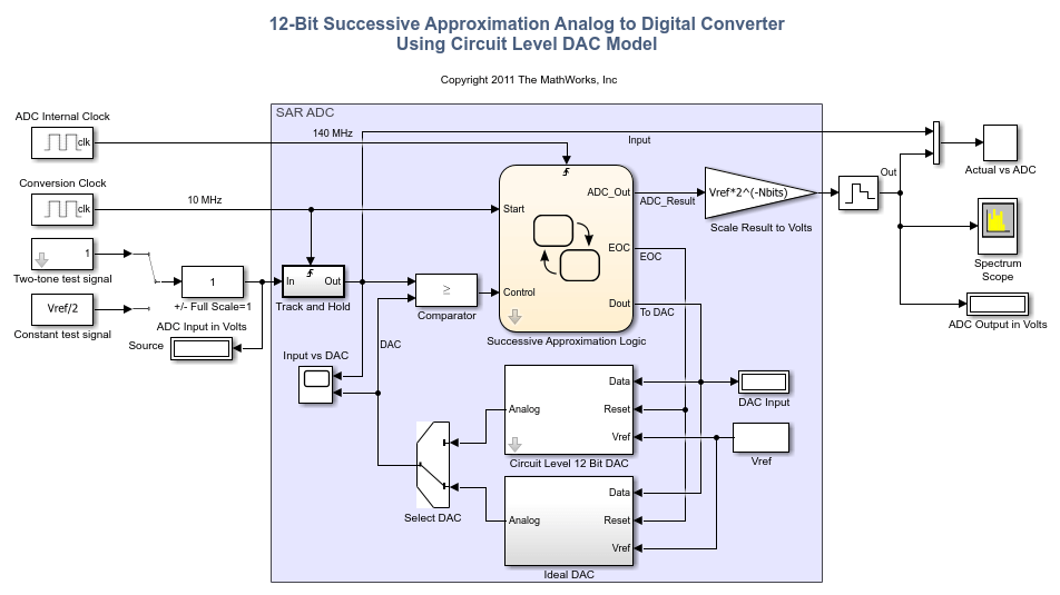
Open the system MSADCSuccessiveApproximation.
model = "MSADCSuccessiveApproximation";
open_system(model)
Set the switches to their default positions, selecting the two-tone source and the ideal DAC model.
set_param(model + "/Source","sw","1");
set_param(model + "/Select DAC","LabelModeActiveChoice","V_2");
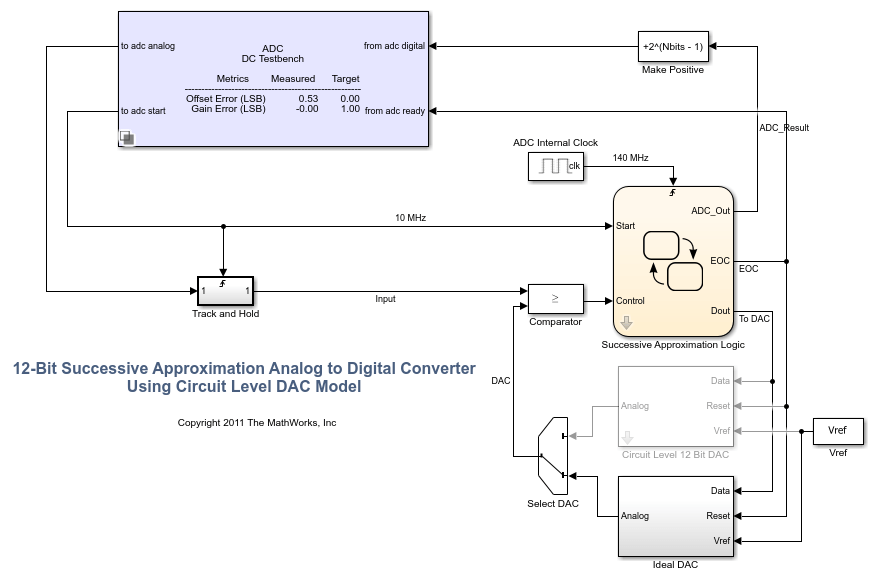
The top-level model consists of a testbench and the device under test. The testbench includes the test signal generators and the time domain scopes and spectrum analyzer for measurement purposes. The device under test, highlighted in blue in the model, contains a Track and Hold:, a Comparator, control logic, and charge scaled DAC.
The test signal is either a two-tone sine wave or a constant DC level input. This test signal is sampled and held at the ADC's output word rate of 10 MHz. The output of the sampler serves as one input to a comparator. The second comparator input is the DAC output which is an incrementally stepped reference level. If the output of the sampler is greater than or equal to the DAC output, then the comparator outputs a logical 1. When this happens, the corresponding bit of the output is set to logical 1. Otherwise, the comparator outputs a logical 0 which does not increment the ADC output word. This single comparator is only place in the successive approximation converter where analog is converted to digital.
sim(model);
Warning: Import Custom Code option will be removed in a future release. Custom
code will be imported by default.
Define the number of bits ( NBits ) and ADC conversion rate ( Fs ) in the MATLAB® workspace. The ADC operating clock rate is determined from Nbits and Fs.
Nbits = 12;
Fs = 1e7;
ADC_clock = Fs*(Nbits+2);
Successive Approximation Control Logic
This model uses Stateflow to model the successive approximation control logic. The state-machine serves as a sequencer that starts by outputting a count corresponding to mid-scale which in this case is 0 volts. The state-machine then performs a binary search of one bit position at a time to find the count corresponding to the closest approximation to the sampled input signal within 12 bits of resolution. The Init state prevents an End of Conversion (EOC) signal from being sent prior to the first conversion.
open_system(model + "/Successive Approximation Logic","force")
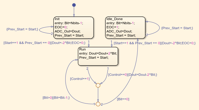
On a particular bit, if the comparator outputs a 1, then that bit is set. Otherwise that bit position is cleared. Because there are 12 bits, it takes 12 clock cycles at the bit rate clock to complete the conversion for a given input sample.
In this model, the bit rate clock denoted by block labeled ADC Internal Clock runs at 140 MHz. This clock is 14 times faster than the sample rate clock denoted by the block labeled Conversion Clock in the upper left corner of the model. After the control logic sequences from bit 11 down to bit 0 the end-of-conversion (EOC) line goes high, telling the DAC circuitry to reset.
DAC Circuit-Level Implementation
The circuit-level DAC uses a multi-stage charge-scaled array of capacitors in a split-array format. This architecture provides several advantages including reduced area or parts count, a built-in sample and hold, low power dissipation, and a relatively small range of capacitance values as would be required without a split-array.
There are two versions of a digital to analog converter (DAC) in this model, one at the circuit-level and the second representing ideal DAC behavior. The ideal DAC block takes the input count and multiplies it by
![$$\frac{V_{ref}}{2^{N_{bits}}} = \frac{2\sqrt{2}}{2^{12}} \left[\frac{Volts}{Count}\right]$$](../../examples/msblks/win64/SuccessiveApproximationADCExample_eq08732127564949006678.png)
to generate the output comparison voltage [1].
Set the switch to enable the circuit-level DAC model. Run the model.
set_param(model + "/Select DAC","LabelModeActiveChoice","V_1");
sim(model);

This particular charge-scaled array uses  binary-weighted capacitors per stage with a total of
  stages providing a total of
  bits of DAC resolution. The binary-weighted capacitors per stage have a value of
  ,
,  , and
, and  . The larger the capacitance corresponds to a higher bit position within a particular stage. For example, setting the low side of the capacitor high has 4 times the output voltage impact relative to setting the low side of the capacitor high.
If you change the value of the variable Nbits, the physical number of bits of the converter, you need to modify the circuit level implementation of the DAC. The ideal DAC implementation and the control logic are parameterized with respect to the number of bits.
open_system(model + "/Circuit Level 12 Bit DAC","force")
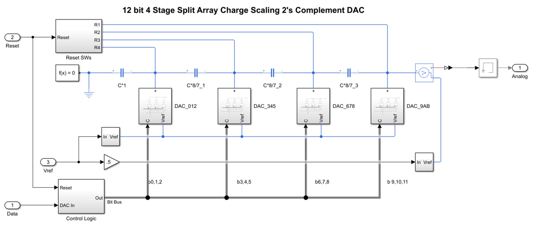
Each stage is separated by a scaling capacitor with value  . The scaling capacitor serves the purpose of attenuating the output voltage of each stage's output voltage. The further the stage is from the DAC output node, the more it is attenuated. The attenuation is 8x per scaling capacitor which corresponds to
  .
.
The three MSBs are closest to the output, bits 0, 1, and 2 while there LSBs, bits 10, 11, and 12 are furthest away. At any given time, the DAC is in one of two modes. It is either generating an output voltage based on a particular input count or it is being reset when the EOC line goes high. When EOC goes high, the low side of each capacitor in the DAC is switched to ground rather than data, thus draining the capacitors of charge in preparation for the next approximation. This effectively drains the capacitive network of charge preparing it for the next input sample.
Measurement Testbench
The ADC Testbench block from the Mixed-Signal Blockset™ can provide a performance analysis of the ADC.
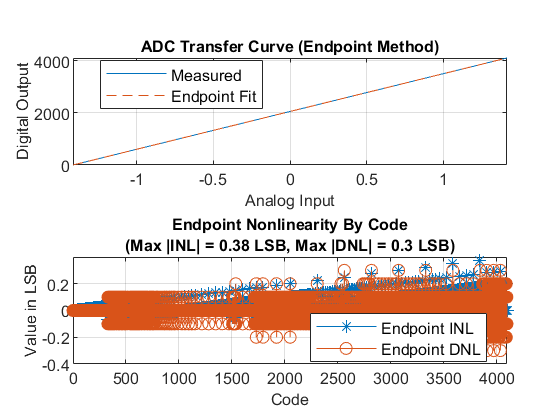
In DC mode, the ADC Testbench tests the linearity of the ADC. The test result is used to generate offset and gain error measurements which are displayed on the block mask. The full test results are available for export or visualization via the buttons on the ADC Testbench block mask.
bdclose(model);
model = "MSADCSAR_DC";
open_system(model);
set_param(model + "/Select DAC","LabelModeActiveChoice","V_2");
sim(model);
Warning: Import Custom Code option will be removed in a future release. Custom
code will be imported by default.
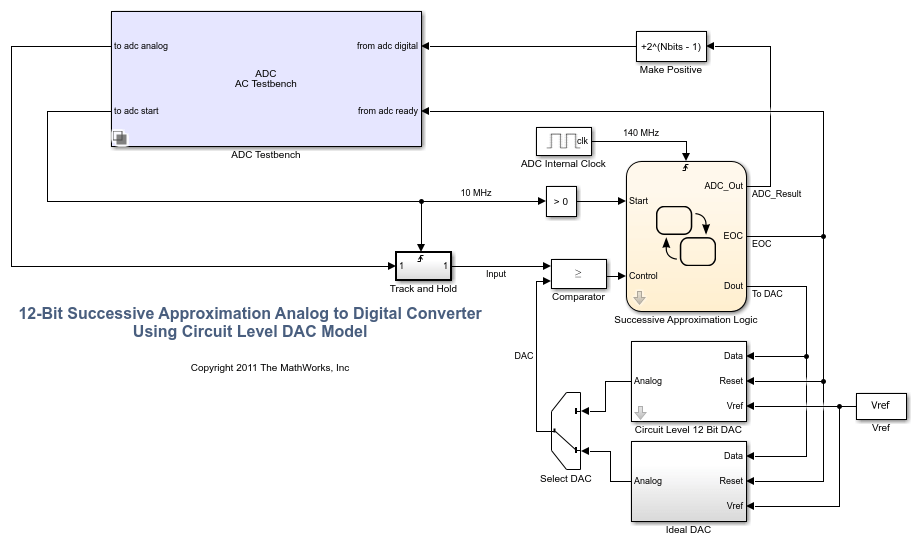
The AC mode of the ADC Testbench provides insight into the frequency performance of the ADC, including measurements like the ENoB (Effective Number of Bits), the maximum measured conversion delay, and the noise floor of the converter. These measurements are displayed on the block icon after simulation and are available for export via a button on the block mask.
model = "MSADCSAR_AC";
open_system(model);
set_param(model + "/Select DAC","LabelModeActiveChoice","V_2");
References
Haideh Khorramabadi UC Berkeley, Department of Electrical Engineering and Computer Sciences, Lecture 15, page 38 <http://inst.eecs.berkeley.edu/~ee247/fa06/lectures/L15_f06.pdf http://inst.eecs.berkeley.edu/~ee247/fa06/lectures/L15_f06.pdf>
Copyright 2019-2020 The MathWorks, Inc. All rights reserved.
See Also
Sampling Clock Source | ADC DC Measurement | ADC AC Measurement